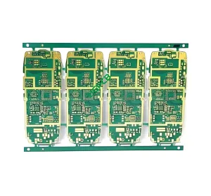
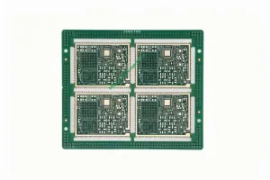
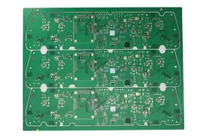
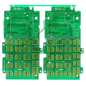
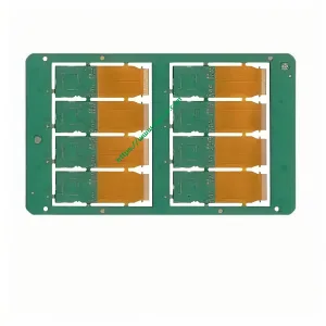
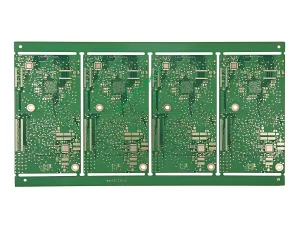
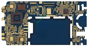
Overview of 8Layers 2+N+2 HDI PCB
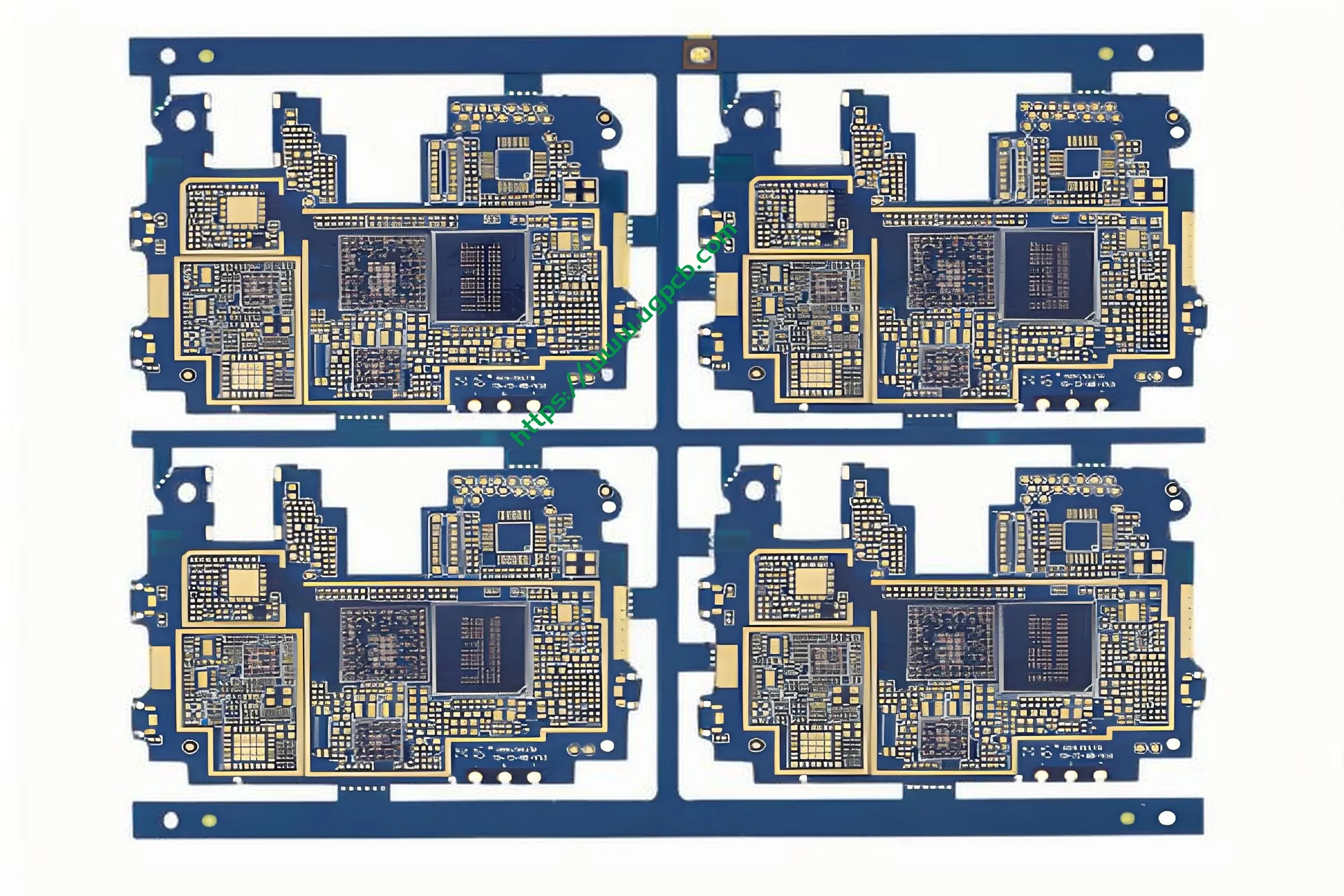
The 8Layers 2+N+2 HDI PCB is a high – density interconnect แผงวงจรพิมพ์. It is a crucial component in modern electronic devices, especially those requiring high – precision circuit connections and advanced functionality.
คำนิยาม
ที่ “8เลเยอร์” refers to the number of signal and power/ground layers in the พีซีบี. “2+ยังไม่มี+2” is a specific layer configuration pattern. “HDI” stands for High – Density Interconnect, which means that this PCB has a high density of traces ( conductive pathways), แผ่นรอง, และจุดแวะ (holes for connection between layers) per unit area compared to PCB ทั่วไป.
ข้อกำหนดการออกแบบ
- ติดตามและพื้นที่: The minimum trace and space is 3mil/3mil, which requires precise design to ensure there is enough space between adjacent traces to avoid electrical interference and short – วงจร.
- ขนาดรู: There are strict requirements for hole sizes. Mechanical holes should be at least 0.2mm in diameter, and laser holes at least 0.1mm. This is to accommodate the placement of components and ensure proper electrical connections.
หลักการทำงาน
Electrical signals are transmitted through the copper traces on different layers of the PCB. The vias connect the corresponding traces on different layers, allowing for complex circuitry to be implemented in a relatively small space. The power and ground layers help to distribute power evenly and reduce electromagnetic interference.
การใช้งาน
One of the main applications is in hand – held electronic equipment PCBs. In devices such as smartphones, แท็บเล็ต, and wearable gadgets, the 8Layers 2+N+2 HDI PCB can handle multiple functions simultaneously, such as communication, กำลังประมวลผล, and sensor interfacing, due to its high – density layout.

การจำแนกประเภท
It can be classified as a multi – layer PCB within the HDI PCB category, with a specific layer architecture of 8 layers following the 2+N+2 pattern.
วัสดุ
The material used is ศ – 4, which is a common fiberglass – reinforced epoxy – วัสดุลามิเนต. It provides good mechanical strength, ฉนวนไฟฟ้า, และความต้านทานความร้อน.
ผลงาน
- ประสิทธิภาพไฟฟ้า: With the inner copper thickness of 1OZ and outer 0.5OZ, it can efficiently transmit electrical signals. The immersion gold surface treatment also has good electrical conductivity and helps to improve the solderability of components.
- สมรรถนะทางกล: The FR – 4 material gives it sufficient mechanical stability to withstand normal handling and installation in electronic devices.
โครงสร้าง
It consists of 8 layers in total. The two outer layers may be used for signal or power/ground connections, ในขณะที่ “n” layer in the middle can be a flexible combination of signal and power/ground layers according to specific design requirements.
คุณสมบัติ
- สูง – ความหนาแน่น: Allows for more components to be mounted on a smaller area.
- Good Surface Treatment: Immersion gold treatment provides good corrosion resistance and solderability.
- Flexible Layer Configuration: The 2+N+2 pattern can be customized to meet different circuit design needs.
กระบวนการผลิต
- เลเยอร์สแต็ค – ขึ้น: Arrange the 8 layers according to the 2+N+2 pattern, ensuring proper alignment.
- การขุดเจาะ: Create mechanical holes and laser holes as per the design requirements.
- การสะสมของทองแดง: Deposit copper in the holes and on the surface to form conductive pathways.
- การแกะสลัก: Remove excess copper to create the desired trace patterns.
- การรักษาพื้นผิว: Apply the immersion gold treatment.
- การจบ: Polish and inspect the PCB to ensure it meets the มาตรฐานคุณภาพ.

สถานการณ์การใช้งาน
As mentioned earlier, it is widely used in hand – held electronic equipment. It can also be used in some small – form – factor computing devices or portable medical devices where space is limited but high – quality circuit connections are required.