

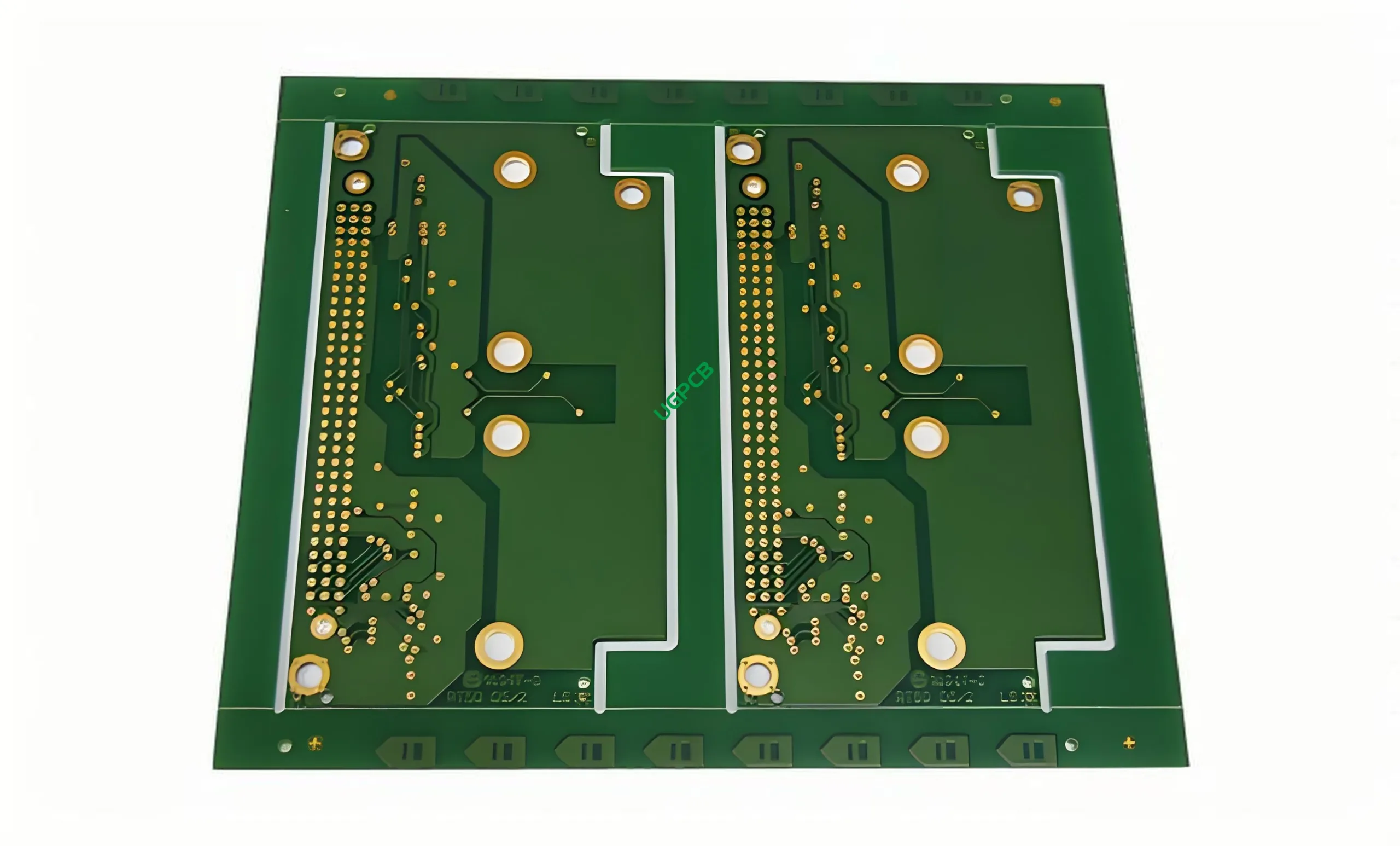
Overview of the 36-Layer High TG Backplane PCB
The 36-Layer High TG Backplane PCB is a high-density, multilayer printed circuit board (พีซีบี) designed for backplane applications. นี้ พีซีบี is ideal for complex electronic systems that need to manage high power and signal integrity.
What is a 36-Layer High TG Backplane PCB?
A 36-Layer High TG Backplane PCB is a printed circuit board (พีซีบี) กับ 36 layers of conductive material separated by insulating layers, specifically designed for backplane applications. คำว่า “High TG” refers to the glass transition temperature, indicating the PCB’s ability to withstand high temperatures without losing its mechanical and electrical properties.
ข้อกำหนดการออกแบบ
The design requirements for a 36-Layer High TG Backplane PCB are stringent to ensure its performance and reliability:
- วัสดุ: TG FR4 สูง, chosen for its excellent electrical and thermal properties.
- จำนวนเลเยอร์: 36 layers to accommodate complex and dense circuit designs.
- สี: Green/White for easy identification and aesthetic appeal.
- ความหนาสำเร็จรูป: 2.4mm to provide structural integrity and durability.
- ความหนาของทองแดง: 1OZ to ensure adequate conductivity and heat dissipation.
- การรักษาพื้นผิว: การแช่ทองคำเพื่อเพิ่มความสามารถในการบัดกรีและความต้านทานการกัดกร่อน.
- Minimum Trace and Space: 4MIL(0.1มม) to support fine circuit patterns.
- ลักษณะเฉพาะ: หลายชั้นสูง, Panasonic M6 PCB material, known for its high reliability and performance.
มันทำงานอย่างไร?
The 36-Layer High TG Backplane PCB works by providing a platform for various electronic components to be interconnected through conductive pathways. These pathways, or traces, are made of copper and are etched onto the board. The high TG FR4 material ensures that the PCB can withstand high temperatures without losing its mechanical and electrical properties, while the immersion gold surface treatment ensures that these traces remain conductive and resistant to corrosion.
การใช้งาน
The primary application of the 36-Layer High TG Backplane PCB is in backplane applications where it manages and regulates the flow of electrical signals. This includes:
- Data communication devices
- อุปกรณ์เครือข่าย
- Industrial control systems
- โครงสร้างพื้นฐานโทรคมนาคม

การจำแนกประเภท
ขึ้นอยู่กับคุณสมบัติและแอปพลิเคชัน, the 36-Layer High TG Backplane PCB can be classified as a high-speed digital PCB designed for backplane applications. This classification highlights its capability to handle high-frequency signals and provide stable electrical connections.
องค์ประกอบของวัสดุ
The core วัสดุ used in the 36-Layer High TG Backplane PCB is High TG FR4, a high-performance composite material known for its excellent mechanical, ความร้อน, และคุณสมบัติไฟฟ้า. This material ensures that the PCB can withstand the demands of backplane applications.
ลักษณะประสิทธิภาพ
The performance characteristics of the 36-Layer High TG Backplane PCB include:
- ความสมบูรณ์ของสัญญาณสูง
- การสูญเสียสัญญาณต่ำ
- การจัดการความร้อนที่เหนือกว่า
- Robust mechanical strength
- Long-term stability
รายละเอียดโครงสร้าง
The structural details of the 36-Layer High TG Backplane PCB are as follows:
- จำนวนเลเยอร์: 36 ชั้น
- ความหนาสำเร็จรูป: 2.4มม
- ความหนาของทองแดง: 1ออนซ์
- การรักษาพื้นผิว: ทองแช่
- Minimum Trace and Space: 4MIL(0.1มม)
- ลักษณะเฉพาะ: หลายชั้นสูง, Panasonic M6 PCB material
คุณสมบัติและประโยชน์
The key features and benefits of the 36-Layer High TG Backplane PCB include:
- การเชื่อมต่อระหว่างกันที่มีความหนาแน่นสูง
- ความสมบูรณ์ของสัญญาณที่ยอดเยี่ยม
- การก่อสร้างเชิงกลที่แข็งแกร่ง
- ประสิทธิภาพระยะยาวที่เชื่อถือได้
- ตัวเลือกสีสุนทรียศาสตร์ (สีเขียว/ขาว)
กระบวนการผลิต
The production process of the 36-Layer High TG Backplane PCB involves several steps including:
- การเลือกวัสดุ: Choosing high-quality High TG FR4 material.
- การซ้อนชั้น: การจัดเรียง 36 เลเยอร์ที่มีความแม่นยำ.
- การแกะสลัก: การลบทองแดงส่วนเกินเพื่อสร้างรูปแบบการติดตามที่ต้องการ.
- แอปพลิเคชันมาสก์ประสาน: Applying a solder mask layer to protect the copper traces.
- การชุบ: การใช้การรักษาพื้นผิวทองคำแบบแช่.
- การประกอบ: การรวม PTHS และ VIAS สำหรับการเชื่อมต่อของเลเยอร์.
- การทดสอบ: ทำให้มั่นใจได้ว่า PCB ตรงตามข้อกำหนดประสิทธิภาพทั้งหมด.
ใช้เคส
The 36-Layer High TG Backplane PCB is used in various scenarios such as:
- Backplane applications in data centers
- High-speed networking equipment
- ระบบอัตโนมัติทางอุตสาหกรรม
- โครงสร้างพื้นฐานโทรคมนาคม


