ภาพรวมของแผงวงจรพิมพ์ LED P2.9
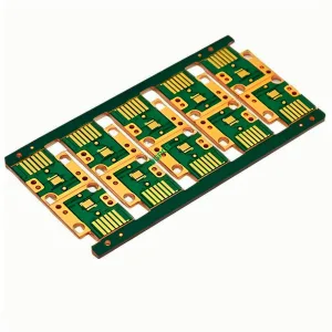
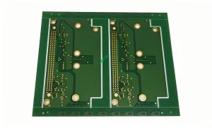
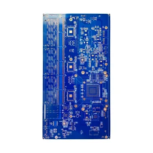
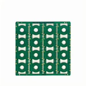
แผงวงจรพิมพ์ LED P2.9 (พีซีบี) เป็นผู้เชี่ยวชาญ พีซีบี ออกแบบมาเพื่อใช้กับโมดูล LED P2.9, ซึ่งมักใช้ในแอพพลิเคชั่นแสดงผลที่มีความละเอียดสูง. PCB นี้เหมาะสำหรับการสร้างขนาดใหญ่, จอแสดงผล LED ไร้รอยต่อ.
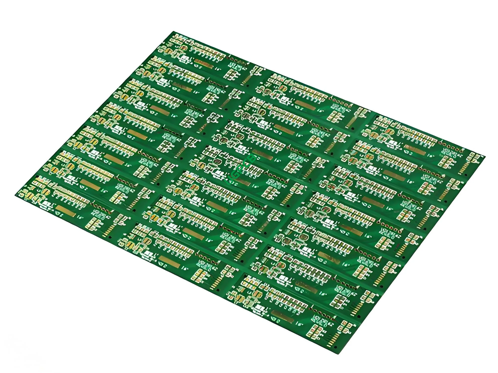
แผงวงจรพิมพ์ LED P2.9 คืออะไร?
แผงวงจรพิมพ์ LED P2.9 คือ แผงวงจรพิมพ์ (พีซีบี) ออกแบบมาโดยเฉพาะเพื่อรองรับและเชื่อมต่อโมดูล LED P2.9. คำว่า “หน้า 2.9” หมายถึงระยะพิทช์พิกเซลของโมดูล LED, ซึ่งมาตรการ 2.9 มิลลิเมตรระหว่างแต่ละพิกเซล. PCB นี้ช่วยให้แน่ใจว่าโมดูล LED สามารถเชื่อมต่อถึงกันได้อย่างมีประสิทธิภาพ, เป็นแพลตฟอร์มที่มั่นคงสำหรับชิ้นส่วนอิเล็กทรอนิกส์.
ข้อกำหนดการออกแบบ
ข้อกำหนดการออกแบบสำหรับแผงวงจรพิมพ์ LED P2.9 นั้นเข้มงวดเพื่อให้มั่นใจถึงประสิทธิภาพและความน่าเชื่อถือ:
- วัสดุ: SY1000-2 TG170 FR4, เลือกเนื่องจากคุณสมบัติทางไฟฟ้าและความร้อนที่ดีเยี่ยม.
- จำนวนเลเยอร์: 6 เพื่อรองรับวงจรที่จำเป็นและความสมบูรณ์ของสัญญาณ.
- สี: สีดำ/ขาวเพื่อให้แยกแยะได้ง่ายและสวยงาม.
- ความหนาสำเร็จรูป: 1.0มม. เพื่อให้โครงสร้างมีความสมบูรณ์และทนทาน.
- ความหนาของทองแดง: 1OZ เพื่อให้แน่ใจว่ามีการนำไฟฟ้าและการกระจายความร้อนเพียงพอ.
- การรักษาพื้นผิว: การแช่ทองคำเพื่อเพิ่มความสามารถในการบัดกรีและความต้านทานการกัดกร่อน.
- การติดตามขั้นต่ำและพื้นที่: 4MIL(0.1มม) เพื่อรองรับรูปแบบวงจรที่ดี.
- ลักษณะเฉพาะ: แผ่นเพิ่มเติมที่มีระยะห่างขนาดเล็กเพื่อรองรับรูปแบบที่หนาแน่นของโมดูล LED P2.9.
มันทำงานอย่างไร?
แผงวงจรพิมพ์ LED P2.9 ทำงานโดยจัดให้มีแพลตฟอร์มสำหรับส่วนประกอบอิเล็กทรอนิกส์ต่างๆ เพื่อเชื่อมต่อถึงกันผ่านทางเดินที่เป็นสื่อกระแสไฟฟ้า. ทางเดินเหล่านี้, หรือร่องรอย, ทำจากทองแดงและสลักลงบนกระดาน. วัสดุ SY1000-2 TG170 FR4 ช่วยให้มั่นใจได้ว่า PCB สามารถทนต่อความต้องการของการใช้งานจอแสดงผล LED, ในขณะที่การรักษาพื้นผิวด้วยทองคำแบบจุ่มช่วยให้แน่ใจว่าร่องรอยเหล่านี้ยังคงเป็นสื่อกระแสไฟฟ้าและทนทานต่อการกัดกร่อน.
การใช้งาน
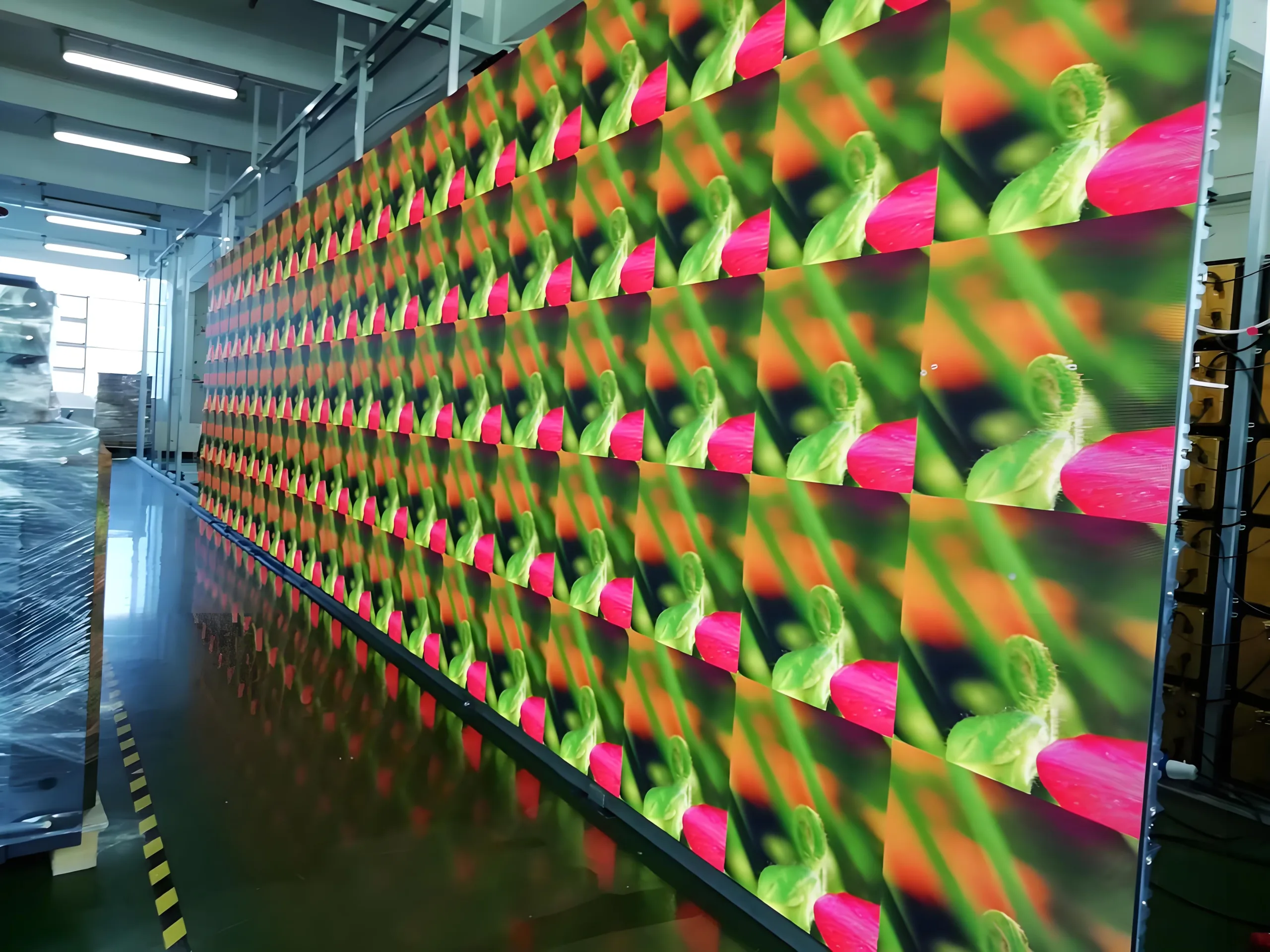
การใช้งานหลักของแผงวงจรพิมพ์ LED P2.9 อยู่ในระบบจอแสดงผล LED ความละเอียดสูง ซึ่งจัดการและควบคุมการไหลของสัญญาณไฟฟ้า. ซึ่งรวมถึง:
- จอแสดงผล LED ในร่มและกลางแจ้ง
- ป้ายดิจิตอล
- ผนังวิดีโอรูปแบบขนาดใหญ่
- เวทีกิจกรรมและหน้าจอคอนเสิร์ต
การจำแนกประเภท
ขึ้นอยู่กับคุณสมบัติและแอปพลิเคชัน, แผงวงจรพิมพ์ LED P2.9 สามารถจัดประเภทได้มีความหนาแน่นสูง, PCB ดิจิตอลความเร็วสูง ออกแบบมาสำหรับการใช้งานจอแสดงผล LED. การจำแนกประเภทนี้เน้นย้ำถึงความสามารถในการจัดการกับสัญญาณความถี่สูงและให้การเชื่อมต่อทางไฟฟ้าที่เสถียร.
องค์ประกอบของวัสดุ
แกนกลาง วัสดุ ที่ใช้ในแผงวงจรพิมพ์ LED P2.9 คือ SY1000-2 TG170 FR4, วัสดุคอมโพสิตประสิทธิภาพสูงซึ่งเป็นที่รู้จักในด้านกลไกที่ยอดเยี่ยม, ความร้อน, และคุณสมบัติไฟฟ้า. วัสดุนี้ช่วยให้แน่ใจว่า PCB สามารถทนต่อความต้องการของการใช้งานจอแสดงผล LED.
ลักษณะประสิทธิภาพ
ลักษณะการทำงานของแผงวงจรพิมพ์ LED P2.9 ประกอบด้วย:
- ความสมบูรณ์ของสัญญาณสูง
- การสูญเสียสัญญาณต่ำ
- การจัดการความร้อนที่เหนือกว่า
- ความแข็งแรงทางกลที่แข็งแกร่ง
- ความมั่นคงในระยะยาว
รายละเอียดโครงสร้าง
รายละเอียดโครงสร้างของแผงวงจรพิมพ์ LED P2.9 มีดังนี้:
- จำนวนเลเยอร์: 6 ชั้น
- ความหนาสำเร็จรูป: 1.0มม
- ความหนาของทองแดง: 1ออนซ์
- การรักษาพื้นผิว: ทองแช่
- การติดตามขั้นต่ำและพื้นที่: 4MIL(0.1มม)
- ลักษณะเฉพาะ: แผ่นเพิ่มเติมที่มีระยะห่างขนาดเล็กเพื่อรองรับรูปแบบที่หนาแน่นของโมดูล LED P2.9.
คุณสมบัติและประโยชน์
คุณสมบัติหลักและคุณประโยชน์ของแผงวงจรพิมพ์ LED P2.9 ประกอบด้วย:
- การเชื่อมต่อระหว่างกันที่มีความหนาแน่นสูง
- ความสมบูรณ์ของสัญญาณที่ยอดเยี่ยม
- การก่อสร้างเชิงกลที่แข็งแกร่ง
- ประสิทธิภาพระยะยาวที่เชื่อถือได้
- ตัวเลือกสีสุนทรียศาสตร์ (ดำ/ขาว)
กระบวนการผลิต
กระบวนการผลิตแผงวงจรพิมพ์ LED P2.9 เกี่ยวข้องกับหลายขั้นตอน ได้แก่:
- การเลือกวัสดุ: การเลือกใช้วัสดุ SY1000-2 TG170 FR4 คุณภาพสูง.
- การซ้อนชั้น: การจัดเรียง 6 เลเยอร์ที่มีความแม่นยำ.
- การแกะสลัก: การลบทองแดงส่วนเกินเพื่อสร้างรูปแบบการติดตามที่ต้องการ.
- แอปพลิเคชันมาสก์ประสาน: การใช้ชั้นหน้ากากประสานเพื่อปกป้องร่องรอยทองแดง.
- การชุบ: การใช้การรักษาพื้นผิวทองคำแบบแช่.
- การประกอบ: การรวม PTHS และ VIAS สำหรับการเชื่อมต่อของเลเยอร์.
- การทดสอบ: ทำให้มั่นใจได้ว่า PCB ตรงตามข้อกำหนดประสิทธิภาพทั้งหมด.
ใช้เคส
แผงวงจรพิมพ์ LED P2.9 ใช้ในสถานการณ์ต่างๆ เช่น:
- จอแสดงผล LED ความละเอียดสูงในร่มและกลางแจ้ง
- การติดตั้งป้ายดิจิตอล
- เวทีคอนเสิร์ตและกิจกรรมต่างๆ พร้อมวิดีโอวอลล์ขนาดใหญ่
- สภาพแวดล้อมการค้าปลีกพร้อมหน้าจอโฆษณาแบบไดนามิก