
Any Layer HDI PCB: The Most Complex Design Structure
ภาพรวม
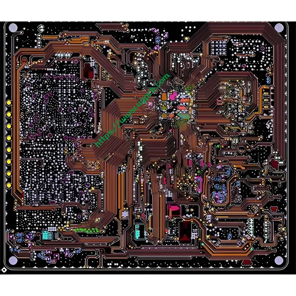
Any Layer HDI PCB is the most complex HDI PCB design structure, offering unparalleled connectivity and performance.
High-Density Interconnect Layers
All Layers as HDI
In this structure, all layers are high-density interconnect layers, allowing for free interconnection of conductors on any layer of the PCB.
Copper-Filled Stacked Microvia Structure
The copper-filled stacked microvia structure facilitates this interconnectivity, providing a reliable and efficient means of connecting various layers.
การใช้งาน
Highly Complex Devices
This structure is ideal for highly complex, high pin-count devices such as CPU and GPU chips used in handheld and mobile devices.
Excellent Electrical Characteristics
The design yields excellent electrical characteristics, making it suitable for high-performance applications.
ประโยชน์
Reliable Interconnect Solution
The Any Layer HDI PCB structure provides a reliable interconnect solution for complex devices, ensuring stable and efficient performance.
UGPCB Advantage
This structure, featuring UGPCB technology, represents a significant advancement in PCB design and manufacturing.


