
Extraordinary Versatility
HDI boards are ideal when weight, ช่องว่าง, ความน่าเชื่อถือ, and performance are the main concerns.
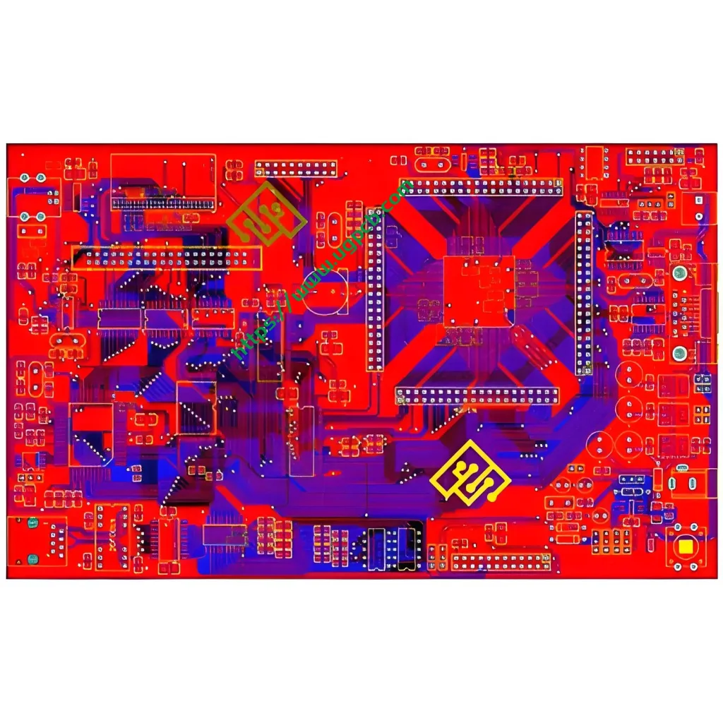
Compact Design
Combination of Blind, Buried, and Micro Vias
The combination of blind, buried, and micro vias reduces board space requirements.
Better Signal Integrity
Via-in-Pad and Blind Via Technology
HDI utilizes via-in-pad and blind via technology, which helps keep components close to each other, reducing signal path lengths.
Removal of Through-hole Stubs
HDI technology removes through-hole stubs, reducing signal reflections and improving signal quality.
Shorter Signal Paths
Due to shorter signal paths, HDI significantly improves signal integrity.
ความน่าเชื่อถือสูง
Stacked Vias
The implementation of stacked vias makes these boards a super barrier against extreme environmental conditions.
Cost-effective
The functionality of a standard 8-layer through-hole board (standard PCB) can be reduced to a 6-layer HDI board without compromising quality.


