
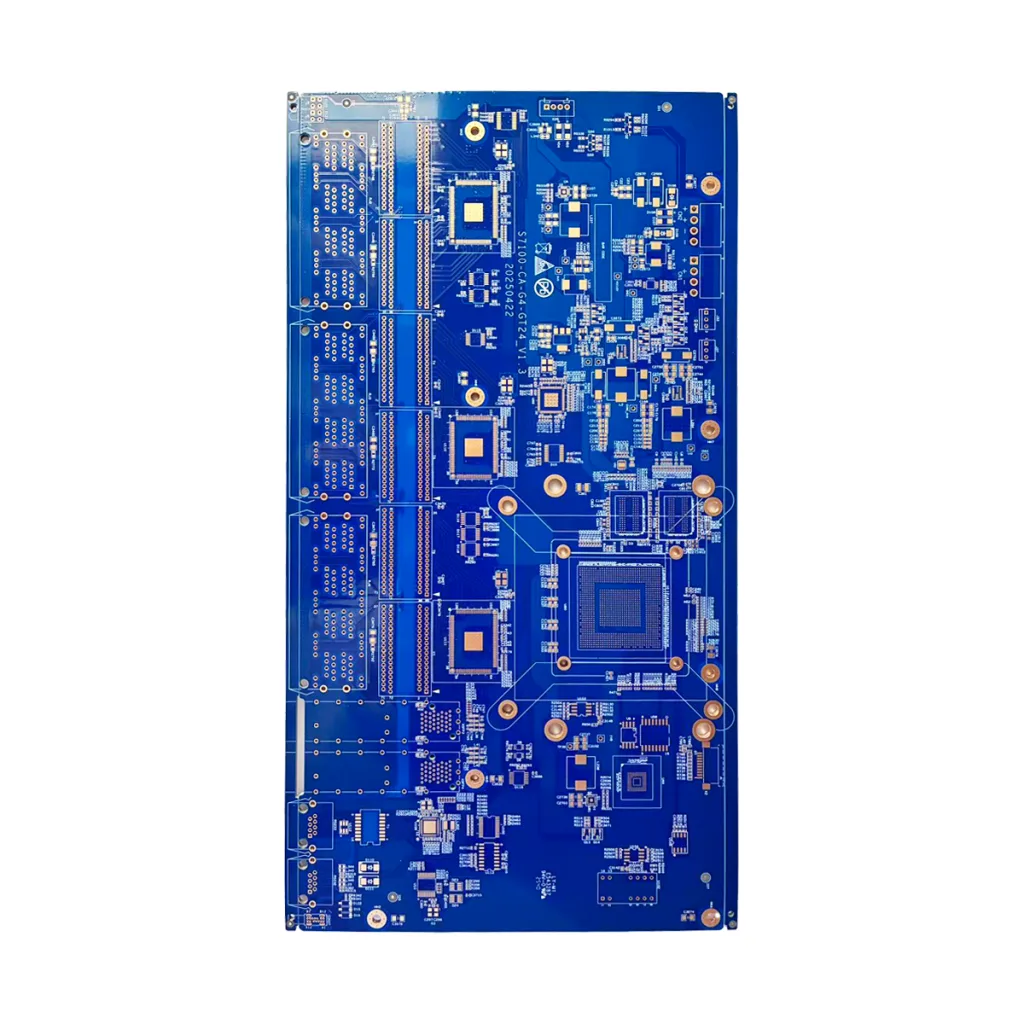

Overview of the Blue Solder Mask PCB
The Blue Solder Mask PCB is a high-density, multilayer printed circuit board (พีซีบี) designed for digital applications requiring mass production. นี้ พีซีบี is ideal for complex electronic systems that need to manage high power and signal integrity.

What is a Blue Solder Mask PCB?
A Blue Solder Mask PCB is a printed circuit board (พีซีบี) with a blue solder mask layer, which is used to protect the copper traces from oxidation and short circuits. The blue color makes it easy to distinguish different ส่วนประกอบ and layers during assembly and inspection.
ข้อกำหนดการออกแบบ
The design requirements for a Blue Solder Mask PCB are stringent to ensure its performance and reliability:
- วัสดุ: FR4, chosen for its excellent electrical and thermal properties.
- จำนวนเลเยอร์: 6 layers to accommodate complex and dense circuit designs.
- สี: สีน้ำเงิน/ขาวเพื่อการระบุได้ง่ายและดึงดูดความงาม.
- ความหนาสำเร็จรูป: 1.2mm to provide structural integrity and durability.
- ความหนาของทองแดง: 1/0.5/0.5/0.5/0.5/1 OZ to ensure adequate conductivity and heat dissipation.
- การรักษาพื้นผิว: การแช่ทองคำเพื่อเพิ่มความสามารถในการบัดกรีและความต้านทานการกัดกร่อน.
- Minimum Trace and Space: 4MIL(0.1มม) to support fine circuit patterns.
มันทำงานอย่างไร?
The Blue Solder Mask PCB works by providing a platform for various electronic components to be interconnected through conductive pathways. These pathways, or traces, are made of copper and are etched onto the board. The blue solder mask layer protects the copper traces from environmental factors, while the immersion gold surface treatment ensures that these traces remain conductive and resistant to corrosion.
การใช้งาน
The primary application of the Blue Solder Mask PCB is in digital electronics where it manages and regulates the flow of electrical signals. This includes:
- Digital signal processors
- Microcontrollers
- โมดูลหน่วยความจำ
- Data communication devices
การจำแนกประเภท
ขึ้นอยู่กับคุณสมบัติและแอปพลิเคชัน, the Blue Solder Mask PCB can be classified as a high-speed digital PCB designed for mass production. This classification highlights its capability to handle high-frequency signals and provide stable electrical connections.
องค์ประกอบของวัสดุ
The core วัสดุ used in the Blue Solder Mask PCB is FR4, a high-performance composite material known for its excellent mechanical, ความร้อน, และคุณสมบัติไฟฟ้า. This material ensures that the PCB can withstand the demands of digital applications.
ลักษณะประสิทธิภาพ
The performance characteristics of the Blue Solder Mask PCB include:
- ความสมบูรณ์ของสัญญาณสูง
- การสูญเสียสัญญาณต่ำ
- การจัดการความร้อนที่เหนือกว่า
- Robust mechanical strength
- Long-term stability
รายละเอียดโครงสร้าง
The structural details of the Blue Solder Mask PCB are as follows:
- จำนวนเลเยอร์: 6 ชั้น
- ความหนาสำเร็จรูป: 1.2มม
- ความหนาของทองแดง: 1/0.5/0.5/0.5/0.5/1 ออนซ์
- การรักษาพื้นผิว: ทองแช่
- Minimum Trace and Space: 4MIL(0.1มม)
คุณสมบัติและประโยชน์
The key features and benefits of the Blue Solder Mask PCB include:
- การเชื่อมต่อระหว่างกันที่มีความหนาแน่นสูง
- ความสมบูรณ์ของสัญญาณที่ยอดเยี่ยม
- การก่อสร้างเชิงกลที่แข็งแกร่ง
- ประสิทธิภาพระยะยาวที่เชื่อถือได้
- ตัวเลือกสีสุนทรียศาสตร์ (สีน้ำเงิน/ขาว)
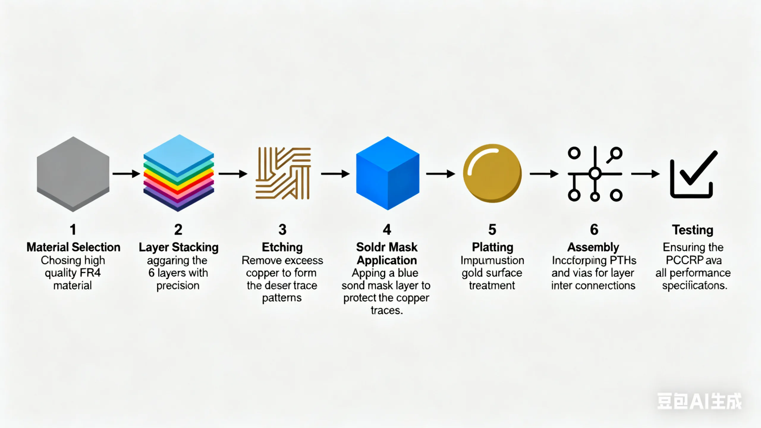
กระบวนการผลิต
The production process of the Blue Solder Mask PCB involves several steps including:
- การเลือกวัสดุ: Choosing high-quality FR4 material.
- การซ้อนชั้น: การจัดเรียง 6 เลเยอร์ที่มีความแม่นยำ.
- การแกะสลัก: การลบทองแดงส่วนเกินเพื่อสร้างรูปแบบการติดตามที่ต้องการ.
- แอปพลิเคชันมาสก์ประสาน: Applying a blue solder mask layer to protect the copper traces.
- การชุบ: การใช้การรักษาพื้นผิวทองคำแบบแช่.
- การประกอบ: การรวม PTHS และ VIAS สำหรับการเชื่อมต่อของเลเยอร์.
- การทดสอบ: ทำให้มั่นใจได้ว่า PCB ตรงตามข้อกำหนดประสิทธิภาพทั้งหมด.
ใช้เคส
The Blue Solder Mask PCB is used in various scenarios such as:
- Digital consumer electronics
- Industrial control systems
- Telecommunication equipment
- อุปกรณ์อิเล็กทรอนิกส์ยานยนต์


I gotta favorite this site it seems extremely helpful handy