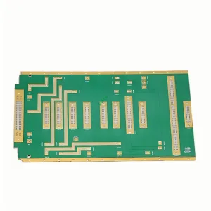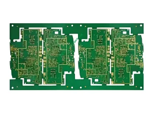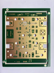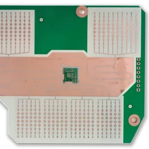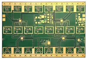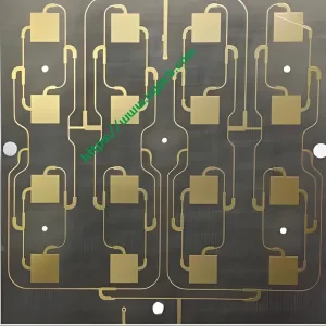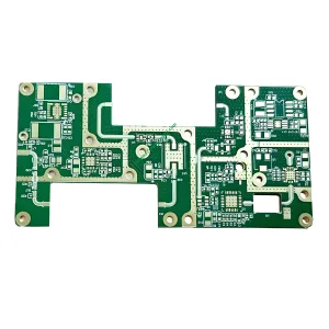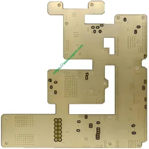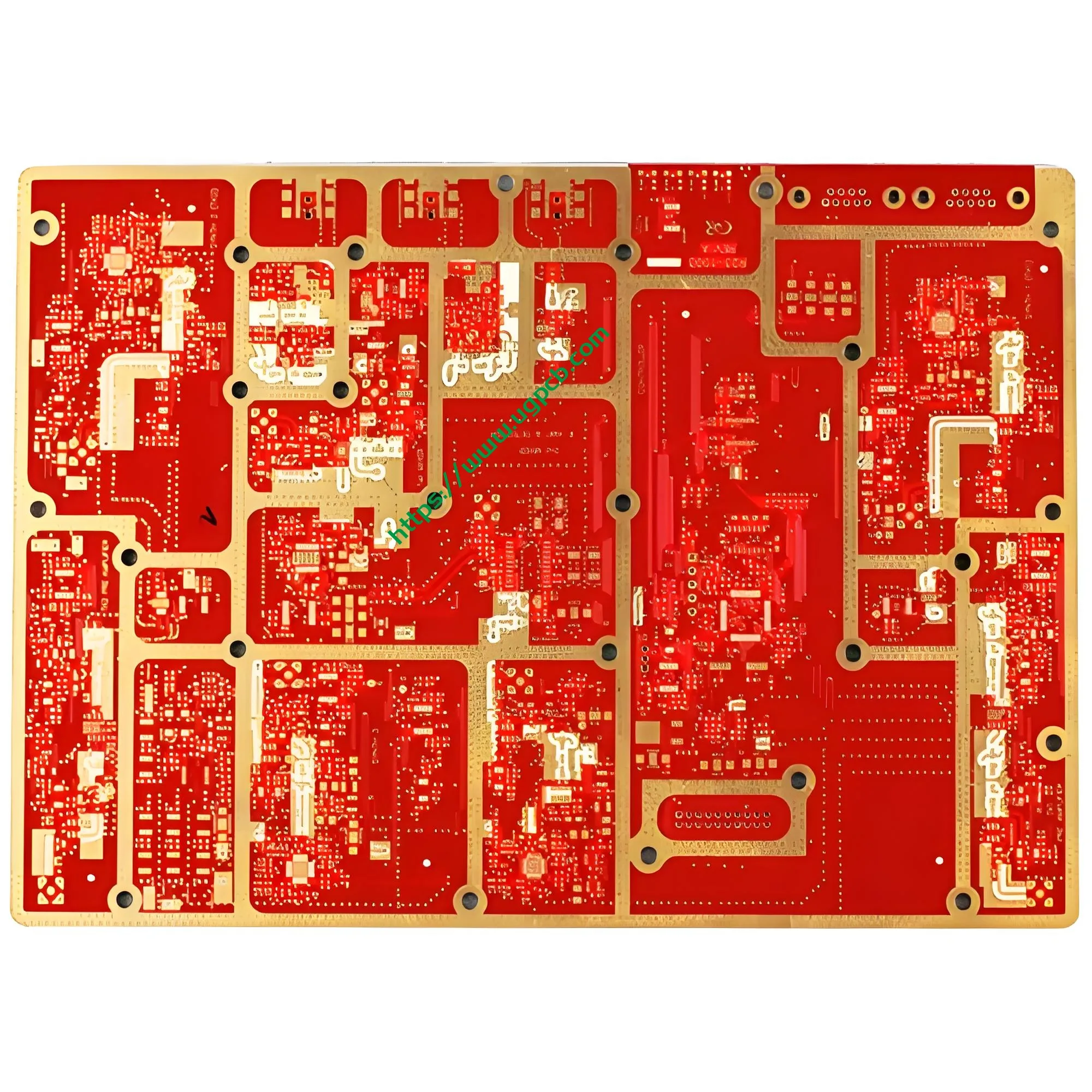
เมื่อระบบดิจิตอลและ RF ดันเกินหลาย GHz, ธรรมดา วัสดุ PCB พบปัญหาคอขวดในความสมบูรณ์ของสัญญาณ, เสถียรภาพทางความร้อน, และ การควบคุมความต้านทาน. PCB ไฮบริดการสื่อสารความถี่สูงของ UGPCB ช่วยแก้ปัญหาความท้าทายเหล่านี้.
1. ภาพรวมผลิตภัณฑ์
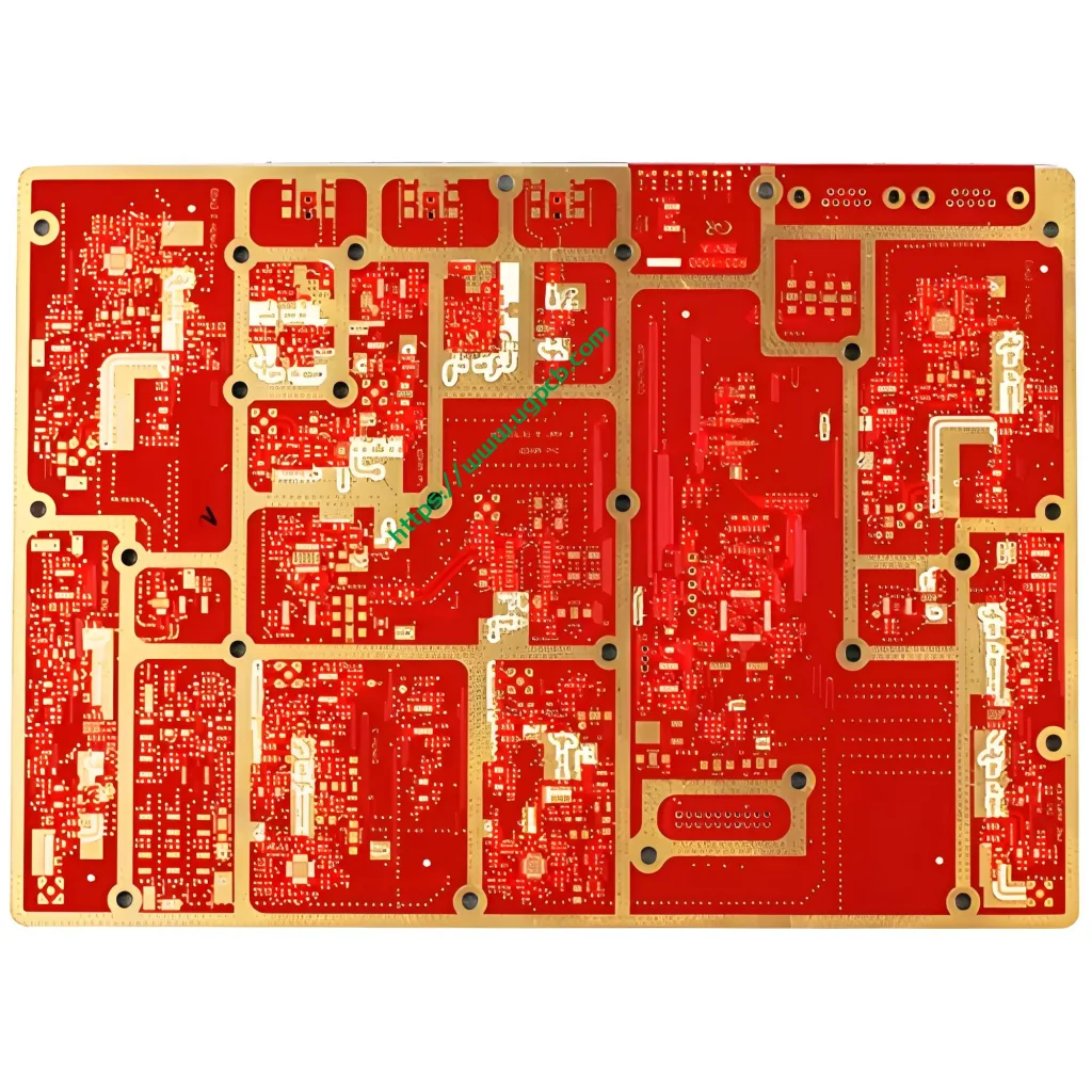
ชื่อสินค้า: UGPCB ไฮบริด PCB ความถี่สูงการสื่อสาร 6 ชั้น
แบบอย่าง: UG‑ไฮบริด‑6L‑RF01
ข้อกำหนดที่สำคัญ: 6 ชั้น / Ro4350B+FR4 อิเล็กทริกผสม / 1.6ความหนาของบอร์ด มม / 210ขนาด มม. × 280 มม / พื้นผิวเคลือบ ENIG / รูเจาะเชิงกลขั้นต่ำ 0.25 มม
การวางตำแหน่ง: โซลูชันการเชื่อมต่อระหว่างกันที่คุ้มค่าสำหรับส่วนหน้า RF และวงจรผสมดิจิทัลความเร็วสูง. โดยการวางลามิเนตความถี่สูง Rogers RO4350B ไว้บนชั้นสัญญาณ RF ด้านบนและ FR-4 ที่ชั้นล่างสุด/กราวด์และเลเยอร์ดิจิทัลความเร็วต่ำ, การออกแบบนี้ช่วยรักษาความสมบูรณ์ของสัญญาณให้สมดุล, เสถียรภาพทางความร้อน, และต้นทุนการผลิต.
2. คำจำกัดความ - PCB ไฮบริดความถี่สูงคืออะไร?
อัน PCB ไฮบริดความถี่สูง (เรียกอีกอย่างว่า คณะกรรมการหลายชั้นอิเล็กทริกผสม) ใช้วัสดุตั้งแต่สองชนิดขึ้นไปที่มีคุณสมบัติเป็นฉนวนต่างกันในหนึ่งเดียว แผงวงจรพิมพ์หลายชั้น.
PCB แบบไฮบริด 6 ชั้นนี้มีสแต็กอัปดังต่อไปนี้:
| ชั้น | การทำงาน | วัสดุ | พารามิเตอร์ที่สำคัญ |
|---|---|---|---|
| L1 | สัญญาณอาร์เอฟ | RO4350B (0.2มม) | Dk=3.48±0.05@10GHz, ฟ=0.0037 |
| L2 | กราวด์ RF | RO4350B | ระนาบอ้างอิงการสูญเสียต่ำ |
| L3 | ดิจิตอลความเร็วสูง | RO4450™ ประสานกัน + FR-4 | การเปลี่ยนแปลง, การจับคู่ความต้านทาน |
| L4 | เครื่องบินพลัง | FR-4 | ค่า Tg สูง, ต้นทุนต่ำ |
| L5 | สัญญาณดิจิตอล | FR-4 | กระจกอีพ็อกซี่มาตรฐาน |
| L6 | กราวด์ดิจิทัล | FR-4 | การสนับสนุนทางกลและการกระจายความร้อน |
“โครงสร้างไดอิเล็กทริกแบบผสมช่วยลดต้นทุนได้อย่างมาก โดยใช้วัสดุความถี่สูงเฉพาะในชั้นที่ส่งสัญญาณ RF เท่านั้น, และ FR-4 สำหรับส่วนที่เหลือ”
3. แนวทางการออกแบบ
3.1 พารามิเตอร์วัสดุที่สำคัญ
สินค้าชิ้นนี้ใช้ Rogers RO4350B (ลามิเนตไฮโดรคาร์บอนที่เติมเซรามิก) และ FR-4. ข้อมูลจำเพาะที่สำคัญของ RO4350B (แหล่งที่มา: เอกสารข้อมูลโรเจอร์ส):
| พารามิเตอร์ | ค่าทั่วไป | สภาพการทดสอบ | อ้างอิง |
|---|---|---|---|
| กระบวนการดีเค | 3.48± 0.05 | 10กิกะเฮิรตซ์ | IPC‑TM‑650 2.5.5.5 |
| ดีเค ดีไซน์ | 3.66 | 10กิกะเฮิรตซ์ | การแก้ไขความหยาบของทองแดง |
| ปัจจัยการกระจาย (ฟ) | 0.0037 | 10กิกะเฮิรตซ์ | แอปพลิเคชัน RF การสูญเสียต่ำ |
| CTE แกน Z | 32 ppm/℃ | -55℃ถึง 288 ℃ | ตรงกับทองแดง (17 ppm/℃) |
| การนำความร้อน | 0.69 w/m · k | 50℃, มาตรฐาน ASTM D5470 | ดีกว่า FR-4 |
| ความติดไฟได้ | อล 94 วี-0 | มาตรฐานยูแอล | สำหรับ RF ที่ใช้งานและกำลังสูง |
แหล่งข้อมูล: เอกสารข้อมูลลามิเนต Rogers Corporation RO4350B™
3.2 การควบคุมความต้านทาน
การควบคุมอิมพีแดนซ์บน PCB แบบไฮบริด 6 ชั้นเป็นเรื่องที่ท้าทายเนื่องจากความไม่ต่อเนื่องของ Dk. ใช้ตัวแก้ปัญหาแม่เหล็กไฟฟ้า 3 มิติ และใช้ปัจจัยการแก้ไขความหยาบของทองแดง (โดยทั่วไปคือ 1.2–1.5). ตามมาตรฐาน IPC‑2141A, ความทนทานต่ออิมพีแดนซ์ลักษณะเฉพาะสำหรับ RF PCB ควรอยู่ภายใน± 7%. UGPCB บรรลุ ±5%.
3.3 การออกแบบซ้อนลามิเนต (ความหนารวม 1.6 มม)
- สูงสุด (L1-L2): RO4350B 0.2มม. × 2 = 0.4 มม
- กลาง (L3): RO4450™ พรีเพก 0.1 มม + แกน FR-4 0.6 มม. = 0.7 มม
- ด้านล่าง (L4-L6): แกน FR-4 + พรีเพรก = 0.5 มม
- ทั้งหมด: 1.6มม
ใช้กราฟแรงกดแบบไดนามิกในระหว่างการเคลือบเพื่อจัดการความเครียดจาก CTE ที่ไม่ตรงกันระหว่าง RO4350B และ FR-4.
4. หลักการทำงาน
ความสมบูรณ์ของสัญญาณ: การสูญเสียอิเล็กทริกมีส่วนสำคัญในการสูญเสียความถี่สูง. ค่าคงที่การลดทอนปานกลางคือ:
ที่ไหน:
- = ค่าคงที่การลดทอนของอิเล็กทริก
- = การอนุญาตแบบสัมพัทธ์ (ค่าการออกแบบ)
- = ความยาวคลื่นในอวกาศว่าง
- = ปัจจัยการกระจาย (ฟ)
RO4350B มี Df = 0.0037 VS. FR-4 0.020. ซึ่งช่วยลดการสูญเสียอิเล็กทริกได้ประมาณ 80%, รับประกันการส่งข้อมูลแบบสูญเสียต่ำสูงสุด 30GHz.
เสถียรภาพทางกลความร้อน: CTE แกน Z ของ RO4350B 32 ppm/℃ ตรงกับทองแดง (17 ppm/℃) ดีกว่า FR-4 มาก (50–70 ppm/℃). สิ่งนี้จะช่วยปรับปรุงการชุบรูทะลุ (พท) ความน่าเชื่อถือภายใต้การหมุนเวียนด้วยความร้อน. ทดสอบตาม IPC‑TM‑650 2.6.7, คณะกรรมการยังมีชีวิตอยู่ 1000 รอบจาก -55°C ถึง 125°C โดยไม่มีการแยกส่วน.
5. แอปพลิเคชันหลัก
PCB ไฮบริดการสื่อสารความถี่สูง 6 ชั้นของ UGPCB ทำหน้าที่หลัก 5 ประการ:
5.1 5สถานีฐานการสื่อสาร G (AAU/RRU)
- คลื่นความถี่: 28GHz และคลื่นมิลลิเมตร 39GHz
- ความต้องการ: การสูญเสียการแทรก < 0.31 เดซิเบล/ซม.@40GHz, การจัดการพลังงาน >200 W/m²@38GHz
- ข้อได้เปรียบ: การก่อสร้างแบบไฮบริดช่วยลดต้นทุนวัสดุลง 30–40% เทียบกับ. วัสดุความถี่สูงทั้งหมด

5.2 77เรดาร์ยานยนต์ GHz/79GHz
- กรณีการใช้งาน: เรดาร์ถ่ายภาพ 4 มิติขับขี่อัตโนมัติ, การตรวจจับจุดบอด, ระบบควบคุมความเร็วคงที่แบบปรับได้
- ความต้องการ: ข้อผิดพลาดของช่วง <0.25เมตรจาก -40 ℃ถึง 125 ℃, ความละเอียดแอซิมัท 0.08°
- ผลงาน: ไอเอ็มเอส 2025 รายงานแสดงความสอดคล้องของเฟส ±0.8° ในช่วงอุณหภูมิเต็มสำหรับโมดูลเรดาร์ไฮบริด 77GHz
5.3 น้ำหนักบรรทุกการสื่อสารผ่านดาวเทียม (เพื่อนร่วมทีม)
- ช่วงความถี่: 17.7 - 31 กิกะเฮิรตซ์
- ข้อได้เปรียบ: 45% การลดน้ำหนักเทียบกับ. พื้นผิวเซรามิกในขณะที่ยังคงประสิทธิภาพ >85%
5.4 ไฟเบอร์ทูเดอะโฮม (FTTH) อุปกรณ์
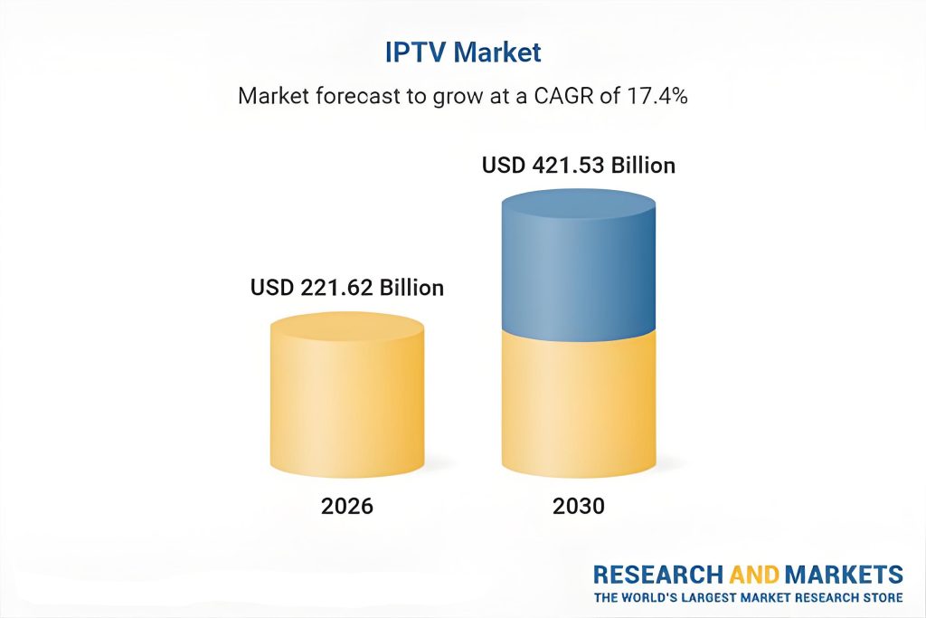
- แนวโน้มตลาด: ตลาด IPTV ทั่วโลกเริ่มต้นที่ 189.25 พันล้านดอลลาร์ (2025) เป็น 421.53 พันล้านดอลลาร์ (2030), cagr 17.4%
- ผลกระทบ: แบนด์วิธสูง, PCB ความหน่วงต่ำถือเป็นสิ่งสำคัญ
5.5 ระบบสัญญาณผสมดิจิตอลความเร็วสูง
- เขตข้อมูล: การถ่ายภาพทางการแพทย์, การตรวจสอบความถี่สูงทางอุตสาหกรรม, สถานีสื่อสารทางทหาร
- ความต้องการ: อยู่ร่วมกัน 10+ สัญญาณดิจิตอล Gbps พร้อมสัญญาณ RF ช่วง GHz
6. การจำแนกประเภททางวิทยาศาสตร์ (สำหรับ IPC-2221)
| มิติการจำแนกประเภท | หมวดหมู่ | พื้นฐาน |
|---|---|---|
| ระบบวัสดุ | PCB อิเล็กทริกผสม | RO4350B + FR-4 |
| ลักษณะความถี่ | RF / ไมโครเวฟ PCB | สูงถึง 30GHz |
| จำนวนชั้น | 6‐บอร์ดหลายชั้น | 6 ชั้นสื่อกระแสไฟฟ้า |
| ความยากทางเทคนิค | การเคลือบไฮบริด HDI | การจับคู่วัสดุที่ไม่ขยายตัว |
| แอปพลิเคชัน | การสื่อสาร RF PCB | โครงสร้างพื้นฐานโทรคมนาคม |
| คลาสประสิทธิภาพของ IPC | คลาส IPC‑6012 3 | อุปกรณ์ที่มีความน่าเชื่อถือสูง |
7. วัสดุในรายละเอียด
7.1 RO4350B ลามิเนตความถี่สูง
- ไฮโดรคาร์บอนเสริมใยแก้ว + ฟิลเลอร์เซรามิก
- ดีเค: 3.48±0.05@10GHz, ค่าสัมประสิทธิ์อุณหภูมิ ~ -50 ppm/℃ (-50℃ถึง +150 ℃)
- ฟ: 0.0037@10GHz
- CTE แกน Z: 32 ppm/℃ – จับคู่ทองแดงเพื่อความน่าเชื่อถือของ PTH
- การนำความร้อน: 0.69 w/m · k (VS. FR-4 0.25–0.35)
- อล 94 วี-0 – เหมาะสำหรับการออกแบบ RF ที่ใช้งานและกำลังสูง
- ความเข้ากันได้ของกระบวนการ: การประมวลผล FR-4 เดียวกัน; ไม่จำเป็นต้องรักษาล่วงหน้าเป็นพิเศษ (ไม่เหมือนไฟเบอร์)
7.2 FR-4 กระจกลามิเนตอีพ็อกซี่
- ผ้าแก้วทอ + อีพอกซีเรซิน
- ดีเค: 4.2–4.8 (1เมกะเฮิรตซ์–1GHz), ฟ: 0.020–0.025
- ค่าใช้จ่าย: 1/5 ถึง 1/10 ของ RO4350B
7.3 RO4450™ แผ่นไม้อัดความถี่สูง
- ชั้นการยึดเหนี่ยวระหว่าง RO4350B และ FR-4
- ดีเค: 3.52±0.05@10GHz (การไล่ระดับสี)
- ฟ: 0.0040@10GHz
7.4 ENIG พื้นผิวสำเร็จรูป (ทองคำแช่นิเกิลแบบไม่ใช้ไฟฟ้า)
- ความหนาของนิกเกิล: 3–6μm (คลาส IPC‑4552 2)
- ทองหนา: 0.05–0.10μm
- ข้อดี: ความสามารถในการบัดกรี, ความเรียบ, ความต้านทานต่อการเกิดออกซิเดชัน, ชุดประกอบ BGA ระดับละเอียด
- มาตรฐาน: ไอพีซี-4552
8. ข้อมูลจำเพาะด้านประสิทธิภาพ
8.1 ประสิทธิภาพไฟฟ้า
| พารามิเตอร์ | ค่า | วิธีทดสอบ |
|---|---|---|
| ความต้านทานลักษณะเฉพาะ (ชั้น RF) | 50โอห์ม ± 5% (ปรับแต่งได้) | IPC-2141A |
| ดีเค (เลเยอร์ RF @10GHz) | 3.48± 0.05 | IPC‑TM‑650 2.5.5.5 |
| การสูญเสียการแทรก | 0.31 เดซิเบล/ซม. @40GHz | สายไมโครสตริป VNA |
| ความเป็นฉนวน | ≥40 กิโลโวลต์/มม | IPC‑TM‑650 2.5.6 |
| ความต้านทานของฉนวน | >10⁹ โอ้ (สภาพปกติ) | IPC‑TM‑650 2.5.17 |
| ทนต่อแรงดันไฟฟ้า | 1000 กระแสตรง, 60ไม่มีพัง | IPC‑TM‑650 2.5.7 |
8.2 สมรรถนะทางกล
| พารามิเตอร์ | ค่า | วิธีทดสอบ |
|---|---|---|
| ความทนทานต่อความหนา | ± 10% | ไอพีซี-6012 |
| ความเสถียรของมิติ | <0.3 มม./ม | IPC‑TM‑650 2.2.4 |
| ความแข็งแรงของเปลือก (1ทองแดง) | ≥1.0 นิวตัน/มม | IPC‑TM‑650 2.4.8 |
| ความแข็งแรงของแรงดัดงอ | ≥350เมกะปาสคาล | IPC‑TM‑650 2.4.4 |
| แรงดึงของแผ่น | ≥5.0 กก./ซม.² | IPC‑TM‑650 2.4.21 |
8.3 ประสิทธิภาพความร้อน
| พารามิเตอร์ | ค่า | วิธีทดสอบ |
|---|---|---|
| ทีจี (พื้นที่ FR-4) | ≥150℃ (TG150) | IPC‑TM‑650 2.4.25 |
| ความเครียดจากความร้อน | 288℃, 10ส × 5 รอบ | IPC‑TM‑650 2.4.13 |
| การปั่นจักรยานด้วยความร้อน | -55℃ ↔ 125 ℃, 1000 รอบ, ไม่มีการปราบปราม | IPC‑TM‑650 2.6.7 |
| การรีโฟลว์แบบไร้สารตะกั่ว | 260℃, 5 รอบ | IPC/JEDEC J-STD-020 |
| ระดับความไวต่อความชื้น | เอ็มเอสแอล 1 | IPC/JEDEC J-STD-020 |
8.4 การรับรองความน่าเชื่อถือ
- คลาส IPC‑6012 3 – อุปกรณ์ที่มีความน่าเชื่อถือสูง
- IPC-6018B – คุณสมบัติสำหรับความถี่สูง (ไมโครเวฟ) PCBS
- อล 94 วี-0
- MIL-PRF-31032 - 1000 รอบความร้อนตั้งแต่ -55 ℃ ถึง 125 ℃
100% การทดสอบไฟฟ้าของโพรบบิน + Aoi. ผลิตภัณฑ์ขั้นสุดท้ายเป็นไปตามคลาส IPC‑A‑600 3.
9. คุณสมบัติเชิงโครงสร้าง
โครงสร้างไฮบริด 6 ชั้นแบบอสมมาตร:
- L1-L2 (RO4350B): ส่วนหน้า RF (ป้า, แอลเอ็นเอ, ตัวกรอง) – โซนวิกฤติความสมบูรณ์ของสัญญาณ
- L3 (การเปลี่ยนแปลง): การจับคู่อิมพีแดนซ์และการเปลี่ยนแปลงชั้นสัญญาณ – แยก RF ออกจากดิจิตอลความเร็วสูง
- L4-L6 (FR-4): การจัดการพลังงาน, การควบคุมแบบดิจิตอล, ส่วนรองรับทางกล – วงจรทั่วไปราคาประหยัด
จบ ENIG: พื้นผิวเรียบช่วยให้มั่นใจได้ถึงการควบคุมอิมพีแดนซ์ที่สม่ำเสมอ. รองรับ BGA, qfn, แพ็คเกจระดับละเอียด. ชั้นทองช่วยปกป้องทองแดงและรับประกันความสามารถในการบัดกรีหลังจากเก็บไว้นาน.
การเจาะที่แม่นยำ & พท: เส้นผ่านศูนย์กลางรูกลขั้นต่ำ 0.25 มม (HDI microvias เหลือ 0.1 มม). ความหนาของทองแดงรู≥20μm (คลาสไอพีซี 3). การบำบัดด้วยพลาสมาด้วยก๊าซผสมต่างๆ สำหรับชั้น RO4350B และ FR-4.
10. ผังกระบวนการผลิต
18 ขั้นตอนสำคัญ:
1 IQC → 2 การสร้างภาพชั้นใน (RF และดิจิตอลแยกกัน) → 3 บราวน์ออกไซด์ → ④ การเปิดใช้งานพลาสมาเบื้องต้น → ⑤ การวางซ้อนแบบไฮบริด → ⑥ การเคลือบด้วยแรงดันสูง (เส้นโค้งความดันไดนามิก) → ⑦ การเจาะเป้าหมายด้วยรังสีเอกซ์ → ⑧ การเจาะด้วยเครื่องกล (0.25mm min) → ⑨ พลาสม่าเดสเมียร์ (รอบคู่) → ⑩ ทองแดงแบบไม่ใช้ไฟฟ้า → ⑪ การถ่ายภาพชั้นนอก → ⑫ การชุบลวดลาย (ทองแดง + ดีบุก) → ⑬ การแกะสลักชั้นนอก (แถบดีบุก) → ⑭ AOI → ⑮ หน้ากากประสาน → ⑯ ENIG → ⑰ การทดสอบทางไฟฟ้า → ⑱ การตรวจสอบขั้นสุดท้าย/บรรจุภัณฑ์
รายละเอียดกระบวนการที่สำคัญ:
- พลาสม่าเคลือบเบื้องต้น (ขั้นตอน 4): CF₄‑N₂‑O₂ สำหรับ FR‑4; ฮีเลียม (เขา) สำหรับ RO4350B
- เส้นโค้งการเคลือบ (ขั้นตอน 6): แรงดันไดนามิก – FR-4 หายก่อน (~180℃), จากนั้นความดันและอุณหภูมิจะเพิ่มขึ้นเป็น> 200 ℃สำหรับ RO4350B
- การขุดเจาะ (ขั้นตอน 8): การจัดการการป้อนขั้นบันไดและอายุการใช้งานของเครื่องมือจะจัดการกับความแตกต่างของความแข็ง
- desmear & พท (ขั้นตอนที่ 9-10): กระบวนการสองรอบเนื่องจากพฤติกรรมทางเคมีที่แตกต่างกัน; รูทองแดง ≥20μm
11. ข้อได้เปรียบในการแข่งขัน
ความสมดุลด้านต้นทุน-ประสิทธิภาพ: ราคาวัสดุ 6 ชั้น RO4350B ทั้งหมด >$200/ตารางเมตร. ไฮบริดใช้ RO4350B เท่านั้น 25% ความหนา →30‐ลดต้นทุนวัสดุ 40%.
ความน่าเชื่อถือ: RO4350B แกน Z CTE = 32 ppm/℃ ตรงกับทองแดง (17 ppm/℃). FR-4 แบบเต็มมี 50-70 ppm/℃. ไฮบริดช่วยลดความเครียด PTH. ผ่าน 1000 รอบ -55 ℃ ถึง 125 ℃ (IPC‑TM‑650 2.6.7).
ความเสถียรของมิติ: CTE ต่ำช่วยลดการบิดเบี้ยว, ปรับปรุงผลผลิต SMT.
| ทิศทาง | RO4350B ซีทีอี | FR-4 CTE (ทั่วไป) |
|---|---|---|
| แกน X | 10 ppm/℃ | 14 ppm/℃ |
| แกน Y | 12 ppm/℃ | 16 ppm/℃ |
| แกน Z | 32 ppm/℃ | 50‐70 ppm/℃ |
เทียบกับ. PTFE เต็ม (เช่น, Rogers RT/Duroid):
| คุณสมบัติ | RO4350B+FR-4 ไฮบริด | PTFE เต็ม |
|---|---|---|
| ความเข้ากันได้ของกระบวนการ | สาย FR-4 มาตรฐาน | อุปกรณ์พิเศษ & การรักษา |
| การทำให้เป็นโลหะ PTH | มาตรฐาน | โซเดียมแนพทาลีนหรือพลาสมา |
| ความเสถียรของมิติ | ยอดเยี่ยม (เสริมด้วยกระจก) | ยากจน, ไหล |
| ค่าใช้จ่าย | 30‐ลดลง 50% | สูง |
12. สรุป & คำแนะนำการสอบถาม
PCB แบบไฮบริดการสื่อสารความถี่สูง 6 ชั้นของ UGPCB เป็นการเชื่อมต่อที่เหมาะสมที่สุดสำหรับระบบสัญญาณผสม RF/ดิจิทัล. ให้บริการสถานีฐาน 5G, เพย์โหลดดาวเทียม Kaband, 77เรดาร์ยานยนต์ GHz, และแอพพลิเคชั่นดิจิตอลความเร็วสูง. โดยการวาง RO4350B บนชั้น RF ที่สำคัญเท่านั้น, เราบรรลุประสิทธิภาพสูงสุดด้วยต้นทุนที่ต่ำกว่ามาก.
สรุปข้อมูลที่สำคัญ:
✅ดค= 3.48 ± 0.05 @10GHz (โรเจอร์สอย่างเป็นทางการ)
✅ ดฟ = 0.0037 @10GHz
✅ แกน Z-TE = 32 ppm/℃ (ตรงกับทองแดง)
✅ การสูญเสียการแทรก ≤ 0.31 เดซิเบล/ซม. @40GHz (ตรวจสอบ IPC‑6018B แล้ว)
✅30‐ลดต้นทุนวัสดุ 40% VS. วัสดุความถี่สูงทั้งหมด
✅ผ่าน 1000 รอบความร้อน -55 ℃ ↔ 125 ℃
ข้อเสนอการสร้างต้นแบบในเวลาจำกัด
โชว์ใบเสนอราคาและข้อเสนอทางเทคนิคที่กำหนดเอง
UGPCB เสนอ 7‐บริการเทิร์นด่วนในวันทำงาน สำหรับ 4-10 ชั้น PCB ไฮบริด. เราจัดให้ การวิเคราะห์ DFM ฟรี.
👉 ส่งไฟล์ Gerber และการออกแบบสแต็กอัพของคุณไปยังอีเมลสนับสนุนทางเทคนิคของเรา. เราจะตอบกลับพร้อมการประเมินทางเทคนิคและใบเสนอราคาที่แม่นยำภายใน 4 ชั่วโมง.
UGPCB – ผู้ผลิต PCB ความถี่สูงแบบไฮบริดที่เชื่อถือได้ของคุณ. จากต้นแบบไปจนถึงการผลิตจำนวนมาก, เรานำเสนอโซลูชันไดอิเล็กตริกผสม 6 ชั้นแบบครบวงจรในที่เดียวเพื่อเร่งความเร็วผลิตภัณฑ์เรดาร์ 5G และผลิตภัณฑ์เรดาร์คลื่นมิลลิเมตรของคุณ.
*แหล่งข้อมูล: เอกสารข้อมูล RO4350B™ ของ Rogers Corporation, มาตรฐาน IPC‑6012D/6018B, วิธีทดสอบ IPC‑TM‑650, จีเอสเอ็มเอ 2026 แนวโน้มโทรคมนาคม, ไอเอ็มเอส 2025 รายงานทางเทคนิคของ International Microwave Symposium*