
High-Density Double-Sided PCB for Consumer Electronics
|With 60-80% higher wiring density than single-sided boards, this 1.6mm double-sided PCB enables more compact and reliable electronic designs.
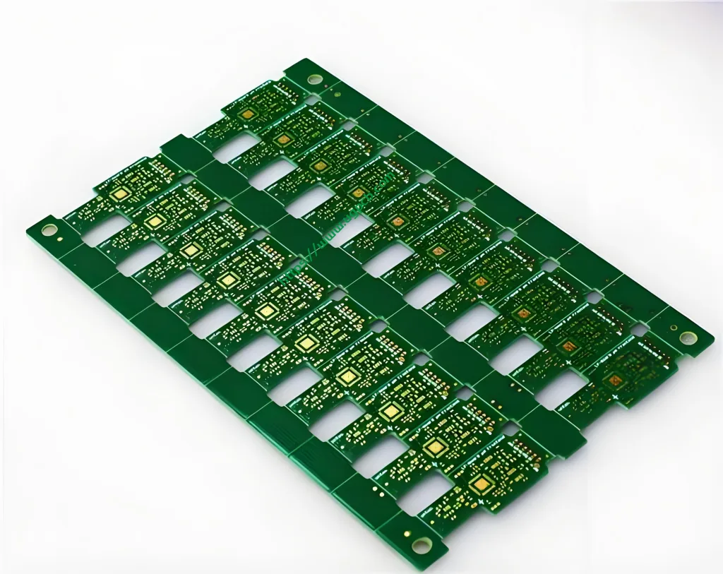
Double-sided แผงวงจรพิมพ์ (PCBS) feature conductive copper layers on both top and bottom sides of an insulating substrate, interconnected by metallized vias. This fundamental architecture is critical for modern, space-constrained electronic devices.
UGPCB’s double-sided PCB utilizes premium KB-6160C FR-4 epoxy glass substrate paired with 1.5OZ finished copper thickness และ ทองแช่ (เห็นด้วย) พื้นผิวเสร็จสิ้น. This combination delivers a robust interconnect solution ideal for consumer electronics, การควบคุมทางอุตสาหกรรม, and telecommunications applications where reliability, ผลงาน, and efficient use of space are paramount.

01 Product Definition & ข้อดีหลัก
A double-sided printed circuit board is a foundational component in modern electronics, providing conductive pathways on both sides of an insulating core.
Electrical connection between the two layers is achieved through metallized through-holes or vias. This design overcomes the spatial limitations inherent to single-sided boards.
For consumer electronics, the flexibility of double-sided PCBs allows for cross-routing and copper pour patterns, which can reduce material costs by 30-50% compared to more complex multi-layer solutions while offering superior design freedom.
The primary structural advantages over single-sided PCBs are dual-sided routing capability และ reliable via-based interlayer conduction. This structure efficiently solves routing congestion issues and supports more complex circuit requirements.
02 ข้อกำหนดวัสดุ: KB-6160C FR-4 Substrate
UGPCB employs KB-6160C FR-4, an epoxy glass cloth copper-clad laminate (CCL) with ultraviolet (UV) blocking functionality.
This substrate is particularly suitable for PCBs requiring simultaneous double-side solder mask curing และ การตรวจสอบด้วยแสงอัตโนมัติ (Aoi).
Key properties of KB-6160C FR-4 include:
-
Excellent Thermal Resistance: High glass transition temperature (ทีจี) for reliable performance during soldering and operation.
-
Superior Mechanical Strength: Enhanced rigidity and dimensional stability compared to standard FR-4 materials.
-
Environmental Compliance: Halogen-free, antimony-free, and red phosphorus-free formulation, meeting stringent environmental safety standards (เช่น, rohs).
03 Operational Principle & การออกแบบโครงสร้าง
The core operational principle of a double-sided PCB is electrical interconnection through metallized vias.
Conductive patterns on both sides of the board are linked via these plated holes, enabling current flow and signal transmission across layers.
The standard stack-up for UGPCB’s 1.6mm double-sided board is as follows:
-
Top Layer: Copper foil (1.5OZ finished thickness)
-
หน้ากากบัดกรี: Green or White (optional)
-
Insulating Core: KB-6160C FR-4 Epoxy Glass Substrate
-
Bottom Layer: Copper foil (1.5OZ finished thickness)
-
พื้นผิวเสร็จสิ้น: ทองแช่ (เห็นด้วย) over Nickel
Via metallization is achieved through a desmear and electrodes copper plating process, typically using either thin-copper electroless deposition with subsequent electrolytic plating or direct metallization transfer for thicker deposits.
04 Precision Manufacturing Process Flow
The manufacturing of double-sided PCBs is more complex than single-sided types, primarily due to the requirements for dual-layer patterning และ reliable via formation. UGPCB’s advanced process flow ensures high quality and consistency.
ที่ Pattern Plating Process is the industry-standard method. The detailed sequence is: Cutting → Drilling → Desmear & Electroless Copper Deposition → Dry Film Lamination & Imaging → Pattern Electroplting → Etching → Solder Mask Application → Legend Printing → Surface Finish (เห็นด้วย) → Profiling/Routing → Electrical Testing → Final Inspection & การบรรจุหีบห่อ.
Electroless Copper Deposition is the critical step for initial via metallization. UGPCB employs a controlled chemical process to deposit a thin, uniform copper layer on the drilled hole walls, which is then electroplated to the specified thickness.
For high-reliability applications, we offer the Solder Mask Over Bare Copper (SMOBC) กระบวนการ. This method enhances solderability, prevents solder bridging on fine-pitch features, and improves shelf life.
05 พื้นผิวเสร็จสิ้น & Key Performance Characteristics
UGPCB specifies ทองแช่ (เห็นด้วย) as the standard surface finish. This provides:
-
Excellent Surface Planarity: Crucial for fine-pitch component soldering.
-
Superior Solderability & Wettability: Ensures reliable solder joints.
-
Low Contact Resistance: Ideal for connectors and gold-finger edges.
-
Long Shelf Life: Resists oxidation better than bare copper or silver finishes.
ที่ 1.5OZ Finished Copper Thickness ensures enhanced current-carrying capacity and improved thermal management compared to standard 1OZ copper. This is vital for power paths and heat dissipation in compact designs.
Technical Advantages Summary:
-
ความคุ้มทุน: Optimal balance between performance and cost for mid-complexity circuits.
-
Design Flexibility: Enables more efficient component placement and routing.
-
ประสิทธิภาพความร้อน: Dual-sided copper aids in heat spreading.
06 Diverse Application Scenarios
Double-sided PCBs, with their balanced performance and cost, are deployed across numerous industries:
อุปกรณ์อิเล็กทรอนิกส์สำหรับผู้บริโภค: Used extensively in smartphones, แท็บเล็ต, แล็ปท็อป, televisions, and audio equipment for mixed-signal (RF/digital) เค้าโครง.
ระบบอัตโนมัติอุตสาหกรรม: Found in control systems, measurement instruments, power supplies, and motor drives due to their reliability and increased current capacity.
โทรคมนาคม: Employed in networking equipment, routers, and base station modules where routing density is key.
Computer Peripherals: Common in printers, scanners, and external storage devices.
07 การประกันคุณภาพ & Technical Compliance
UGPCB implements a rigorous quality management system to ensure every PCB meets exacting standards.
Advanced Manufacturing Equipment: We utilize systems like the LDI for high-precision, double-side simultaneous imaging, achieving registration accuracy within ±12.5μm, which significantly improves production yield.
Specialized Testing: For high-frequency or high-speed designs, we perform additional ความสมบูรณ์ของสัญญาณ (และ) และ การควบคุมความต้านทาน การทดสอบ. Drilling parameters and cleaning processes are strictly controlled to prevent defects like hole voids or insufficient copper.
ด้านสิ่งแวดล้อม & Process Leadership: Our processes adhere to the latest environmental standards. We employ advanced technologies like carbon direct metallization และ conductive polymer deposition as modern, efficient alternatives to traditional chemical copper processes, aligning with ไอพีซี-6012 และ IPC-A-600 acceptability standards.
A circuit designer finalizes the layout, confident that the 1.5OZ copper and robust vias will handle the device’s power needs. Each plated via acts as a microscopic bridge, seamlessly connecting the top and bottom layers, transforming intricate schematics into a stable, functioning electronic system.
As electronics continue their trend toward miniaturization and higher performance, PCB technology is advancing toward trace widths of 25μm (1 MIL) and densities approaching 75% of a four-layer board’s capacity. For engineers facing the dual challenges of space constraints and performance requirements today, the solution may well reside within the layers of this reliable 1.6mm double-sided PCB from UGPCB.


This is very attention-grabbing, You are an excessively professional blogger.I’ve joined your feed and stay up for in quest of extra of your fantastic post. อีกด้วย, I have shared your web site in my social networks。
Hey there fantastic blog! Does running a blog similar