

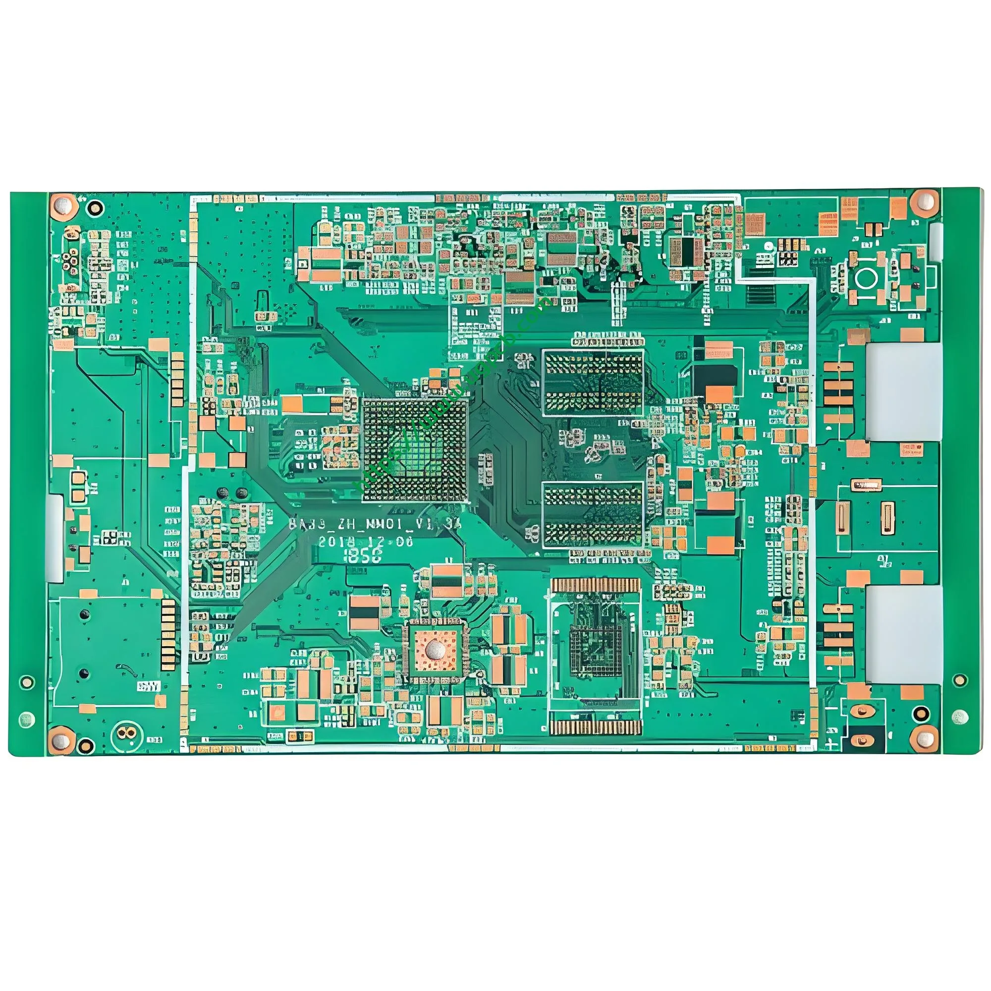
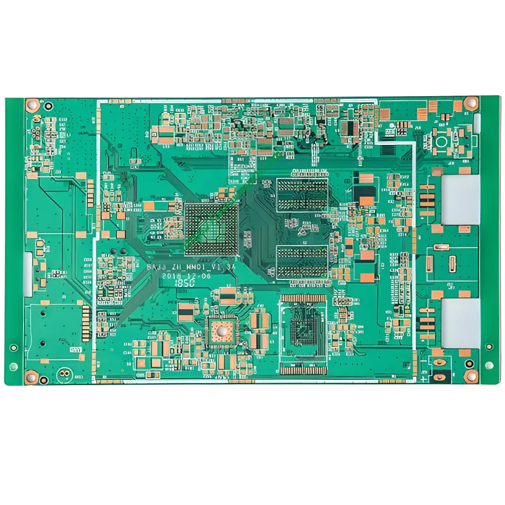
ภาพรวมผลิตภัณฑ์: แผงวงจร PCB สารต้านอนุมูลอิสระ OSP คืออะไร?
หนึ่งแผงวงจร PCB สารต้านอนุมูลอิสระ OSP การใช้งานสารกันบูดที่สามารถบัดกรีได้แบบอินทรีย์ (โอป) เป็นพื้นผิวทองแดง. กระบวนการนี้จะสะสมฟิล์มอินทรีย์บางพิเศษไว้บนพื้นผิวทองแดงเปลือย. ฟิล์มป้องกันการเกิดออกซิเดชันระหว่างการเก็บและการประกอบ. ระหว่างการบัดกรี, ฟลักซ์จะละลายฟิล์ม OSP อย่างรวดเร็ว. สิ่งนี้ทำให้ทองแดงสะอาดสำหรับข้อต่อบัดกรีที่เชื่อถือได้.
ใช้แผงวงจร PCB สารต้านอนุมูลอิสระ OSP ของ UGPCBลามิเนตอีพ็อกซี่แก้ว FR-4 เป็นวัสดุฐาน. มีขนาด 35μm (1 ออนซ์) ฟอยล์ทองแดง, 1.6ความหนาของบอร์ด มม, และขนาดของ 68.36 × 34.6มม. ขนาดรูสำเร็จรูปขั้นต่ำคือ 0.45 มม. ความกว้างการติดตามขั้นต่ำคือ 0.15 มม. และระยะห่างขั้นต่ำคือ 0.20 มม. ผลิตภัณฑ์นี้สอดคล้องกับ IPC-6012E อย่างสมบูรณ์ (คุณสมบัติและประสิทธิภาพของบอร์ดพิมพ์ที่เข้มงวด) และไอพีซี-4555 (ประสิทธิภาพ OSP ที่อุณหภูมิสูง) ข้อกำหนด.
นี้OSP PCB สองด้าน ให้บริการเครื่องใช้ไฟฟ้า, อุปกรณ์สื่อสาร, และการควบคุมทางอุตสาหกรรม. ใช้งานได้ดีที่สุดในบริเวณที่ความไวต่อต้นทุนและความเรียบของพื้นผิวมีความสำคัญมากที่สุด.
การจำแนกประเภทผลิตภัณฑ์ทางวิทยาศาสตร์
อิงตามระบบการจำแนก PCB ระหว่างประเทศ, ผลิตภัณฑ์นี้จัดอยู่ในหมวดหมู่เหล่านี้:
| มิติการจำแนกประเภท | หมวดหมู่ |
|---|---|
| วัสดุพื้นผิว | PCB แข็งผ้าแก้วอีพ็อกซี่ FR-4 |
| จำนวนเลเยอร์ | สองด้าน (วงจรสองชั้น) |
| พื้นผิวเสร็จสิ้น | โอป (สารกันบูดที่สามารถบัดกรีได้แบบอินทรีย์) สารต้านอนุมูลอิสระ |
| คะแนนความไวไฟ | อล 94 วี-0 |
| คลาสประสิทธิภาพของ IPC | ระดับ 2 (บริการเฉพาะผลิตภัณฑ์อิเล็กทรอนิกส์) |
| ความหนาของฟอยล์ทองแดง | 1 ออนซ์ (35μm) ทองแดงมาตรฐาน |
| ความหนาของบอร์ด | 1.6กระดานแข็งมาตรฐาน มม |
| ประเภทรู | รูทะลุเข้ากันได้กับ SMT |
อธิบายพารามิเตอร์ทางเทคนิคที่สำคัญ
พื้นผิว: FR-4 ผ้าแก้วอีพ็อกซี่
FR-4 เป็นสารตั้งต้นที่มีความแข็งมากที่สุดใน พีซีบี อุตสาหกรรม. “ศ” หมายถึงสารหน่วงไฟ. “4” บ่งบอกว่าอีพอกซีเรซินผสมกับผ้าแก้วที่เข้ากันอล 94 วี-0 มาตรฐานการติดไฟ. อล 94 วี-0 ต้องใช้ชิ้นงานแนวตั้งเพื่อดับไฟเองภายใน10 ไม่กี่วินาที หลังจากพ่นไฟเป็นเวลา 10 วินาทีสองครั้ง. ไม่มีหยดเพลิงใดที่อาจทำให้ฝ้ายติดไฟได้.

อุณหภูมิการเปลี่ยนสถานะคล้ายแก้ว (ทีจี) วัดความต้านทานความร้อน. FR-4 Tg มาตรฐานมีช่วงอุณหภูมิตั้งแต่ 130–140°C. Mid-Tg FR-4 ถึง 150–160°C. Tg FR-4 สูงเกิน 170°C. ผลิตภัณฑ์นี้ใช้มาตรฐาน FR-4 ที่มี Tg ≥ 130°C (ตรงตามมาตรฐาน IPC-4101/21). สิ่งนี้เป็นไปตามความต้องการการเปลี่ยนแปลงอุณหภูมิของการบัดกรีแบบรีโฟลว์ (อุณหภูมิสูงสุด 240–260°C).
ความหนาของฟอยล์ทองแดง: 35μm (1 ออนซ์)
ความหนาของทองแดงเป็นตัวกำหนดความสามารถในการรับกระแสไฟฟ้า. สินค้าชิ้นนี้ใช้35μm ฟอยล์ทองแดง, รู้จักกันในนาม1 ทองแดง (1 ออนซ์/ฟุต² อยู่ที่ 35μm). อ้างอิงจาก IPC-2221, 1 ทองแดงออนซ์ที่อุณหภูมิเพิ่มขึ้น 10°C มีค่าประมาณ:
- 0.15มม (6 MIL) ความกว้างของการติดตาม: 0.5-0.7A
- 0.20มม (8 MIL) ความกว้างของการติดตาม: 0.8-1.0A
ความหนาของทองแดง 35μm เป็นมาตรฐานทั่วไปที่สุดสำหรับ PCB แบบสองด้าน. มันทำให้ต้นทุนสมดุล, ความจุปัจจุบัน, และผลผลิตการผลิต.
ขนาดบอร์ด: 68.36 × 34.6มม
มาตรการบอร์ดสำเร็จรูป68.36มม. × 34.6 มม. ขนาดกะทัดรัดนี้เหมาะกับโมดูลอิเล็กทรอนิกส์ที่คับแคบ. PCB ขนาดเล็กต้องการความแม่นยำที่เข้มงวดมากขึ้น โดยทั่วไปความคลาดเคลื่อนของขนาดจะอยู่ภายใน ±0.15 มม (คลาส IPC-6012 2).
ขนาดรูสำเร็จรูปขั้นต่ำ: 0.45มม
0.45มม คือค่ารูเจาะทะลุที่ชุบขั้นต่ำ (พท) เส้นผ่านศูนย์กลาง. ขนาดรูนี้เป็นมาตรฐานในอุตสาหกรรม. ช่วยให้มั่นใจได้ถึงการชุบที่เชื่อถือได้ (อัตราส่วนภาพโดยประมาณ 3.6:1 ด้วยความหนากระดาน 1.6 มม). ขนาดรูรองรับส่วนประกอบ DIP ส่วนใหญ่และการออกแบบแผ่น SMT มาตรฐาน.
ความหนาของพีซีบี: 1.6มม
1.6มม คือความหนาของบอร์ดที่พบบ่อยที่สุดในการผลิต PCB. ให้ความแข็งแรงทางกลที่ดีเยี่ยมและความแข็งแกร่งด้านแรงดัดงอ. มันตรงกับขั้วต่อและซ็อกเก็ตมาตรฐานอย่างสมบูรณ์แบบ.
ติดตามความกว้างและระยะห่าง: 0.15มม / 0.20มม
ผลิตภัณฑ์นี้นำเสนอความกว้างรอยขั้นต่ำ 0.15 มม (เกี่ยวกับ 6 ล้าน) และระยะห่างขั้นต่ำ 0.20 มม (เกี่ยวกับ 8 ล้าน). ตามการจำแนกประเภท IPC, มิติเหล่านี้ตกอยู่ในระดับ 2 (บริการเฉพาะผลิตภัณฑ์อิเล็กทรอนิกส์). ความแม่นยำนี้ตรงตามการออกแบบ PCB ความหนาแน่นปานกลางส่วนใหญ่, รวมถึงบอร์ดควบคุม MCU, โมดูลการจัดการพลังงาน, และบอร์ดแปลงอินเทอร์เฟซ.
กระบวนการต้านอนุมูลอิสระของ OSP ทำงานอย่างไร
กระบวนการ OSP จะสร้างฟิล์มอินทรีย์บางพิเศษบนทองแดงเปลือยที่สะอาดผ่านการดูดซับสารเคมี. ภาพยนตร์ OSP ส่วนใหญ่ประกอบด้วยสารประกอบอัลคิลเบนซิมิดาโซล (ที่ใช้เอโซล). ความหนาของฟิล์มโดยทั่วไปจะอยู่ในช่วงตั้งแต่0.2–0.5μm.
กลไกการป้องกัน
ฟิล์ม OSP ปกป้องพื้นผิวทองแดงด้วยกลไก 3 ประการ:
- สิ่งกีดขวางทางกายภาพ – ฟิล์มอินทรีย์ก่อตัวเป็นชั้นโมเลกุลหนาแน่น. ช่วยป้องกันออกซิเจนและความชื้นไม่ให้สัมผัสกับพื้นผิวทองแดง.
- การดูดซับสารเคมี – กลุ่มที่ทำงานอยู่ในโมเลกุล OSP จะเกิดพันธะทางเคมีกับอะตอมของทองแดง. สิ่งนี้จะสร้างการยึดเกาะที่แข็งแกร่ง.
- การป้องกันแบบเลือกสรร – ฟิล์ม OSP ครอบคลุมเฉพาะบริเวณที่เป็นทองแดง. ไม่ส่งผลกระทบต่อหน้ากากประสานหรือบริเวณอื่นที่ไม่ใช่โลหะ.
พฤติกรรมระหว่างการบัดกรี
ระหว่างการรีโฟลว์ SMT, อุณหภูมิถึง190–230°ซ. ส่วนผสมออกฤทธิ์ของฟลักซ์จะสลายตัวและละลายฟิล์ม OSP. ซึ่งจะทำให้ทองแดงสะอาดอยู่ข้างใต้. บัดกรีจะสัมผัสกับทองแดงและแบบฟอร์มโดยตรงสารประกอบระหว่างโลหะ (ไอเอ็มซี). สิ่งนี้จะสร้างการเชื่อมต่อทางไฟฟ้าที่เชื่อถือได้. ภาพยนตร์ OSPสลายตัวอย่างสมบูรณ์ โดยไม่มีสารตกค้างหลังจากการบัดกรี.
ลักษณะประสิทธิภาพที่สำคัญ
อิงตามวิธีทดสอบ IPC-TM-650:
| ลักษณะเฉพาะ | ค่าทั่วไป / ความต้องการ | มาตรฐานอ้างอิง |
|---|---|---|
| ความหนาของฟิล์ม OSP | 0.2–0.5μm | ไอพีซี-4555 |
| มุมเปียกของบัดกรี | ≤30° (หลังจาก 1 รีด) | IPC-TM-650 2.4.1 |
| อัตราส่วนการแพร่กระจายของบัดกรี | ≥80% | IPC-TM-650 2.4.1 |
| การป้องกันการเกิดออกซิเดชัน (โดยรอบ) | ≥6เดือน | ไอพีซี-4555 |
| ติดต่อเปลี่ยนแนวต้าน | ≤10% (หลังจาก 6 การจัดเก็บเดือน) | IPC-TM-650 |
กระบวนการผลิต PCB สารต้านอนุมูลอิสระ OSP
การผลิต PCB สารต้านอนุมูลอิสระ OSP ปฏิบัติตามการควบคุมกระบวนการที่เข้มงวด. ทุกขั้นตอนส่งผลต่อคุณภาพขั้นสุดท้ายและความน่าเชื่อถือ.
กระบวนการส่วนหน้า (การเตรียมพื้นผิว & รูปแบบวงจร)
- การตัดวัสดุ – ตัดลามิเนตหุ้มทองแดง FR-4 ตามขนาด
- การขุดเจาะ – การเจาะ CNC ด้วยขนาดรูขั้นต่ำ 0.45 มม
- ทองแดงแบบไม่ใช้ไฟฟ้า / การชุบด้วยไฟฟ้า – ผนังหลุมเป็นโลหะสำหรับการเชื่อมต่อแบบชั้นต่อชั้น
- การถ่ายโอนรูปแบบวงจร – ฟิล์มแห้ง / การเปิดรับและการพัฒนาของฟิล์มเปียก
- การแกะสลัก – ขจัดทองแดงที่ไม่ต้องการเพื่อสร้างรอยเส้น 0.15 มม / 0.20วงจรระยะห่าง มม
- การพิมพ์หน้ากากประสาน – ใช้หมึกหน้ากากประสานสีเขียวหรือสีอื่น ๆ
- ทำความสะอาดล่วงหน้า – กำจัดออกไซด์และสิ่งปนเปื้อนก่อนการตกแต่งพื้นผิว
กระบวนการเคลือบ OSP (กระบวนการหลัก)
การไหลของการเคลือบ OSP โดยทั่วไป:
การล้างไขมัน → การล้างด้วยน้ำสองครั้ง → การแกะสลักแบบไมโคร → การล้างด้วยน้ำสองครั้ง → การดองด้วยกรด → การล้างน้ำ DI → การสร้างฟิล์ม OSP → การอบแห้งด้วยอากาศ → การล้างน้ำ DI → การอบแห้งขั้นสุดท้าย
- การแกะสลักแบบไมโคร – ขจัดคอปเปอร์ออกไซด์และสร้างพื้นผิวที่หยาบกร้านด้วยกล้องจุลทรรศน์. สิ่งนี้ส่งเสริมการเติบโตของฟิล์ม OSP.
- การก่อตัวของฟิล์ม OSP – จุ่ม PCB ในเคมี OSP (อัลคิล เบนซิมิดาโซล, กรดอินทรีย์, คอปเปอร์คลอไรด์, และน้ำปราศจากไอออน). ฟิล์มเจริญเติบโตได้จากการดูดซับสารเคมีบนพื้นผิวทองแดง.
- การควบคุมความหนาของฟิล์ม – การควบคุมที่แม่นยำเป็นสิ่งสำคัญ. บางเกินไปหมายถึงทนความร้อนได้ไม่ดี. ความหนาเกินไปขัดขวางการทำงานของฟลักซ์และการไหลของบัดกรี.
กระบวนการแบ็คเอนด์
- การกำหนดเส้นทาง – การกำหนดเส้นทาง CNC ไปยังมิติสุดท้าย
- การทดสอบไฟฟ้า – การทดสอบการบินด้วยโพรบหรือฟิกซ์เจอร์
- การตรวจสอบขั้นสุดท้าย – การตรวจสอบด้วยสายตาและการสุ่มตัวอย่างความหนาของฟิล์ม
- บรรจุภัณฑ์สูญญากาศ – บรรจุภัณฑ์ป้องกันความชื้นและป้องกันการเกิดออกซิเดชัน
คุณลักษณะของผลิตภัณฑ์และข้อดีหลัก
ความเรียบของพื้นผิวที่ดีเยี่ยม
ฟิล์ม OSP เท่านั้น0.2–0.5μm หนา. เกิดจากการดูดซับสารเคมีที่มีความหนาสม่ำเสมอและพื้นผิวเรียบ. สิ่งนี้จะรักษาความเรียบของฟอยล์ทองแดงดั้งเดิม. มันเหมาะสำหรับSMT ระดับละเอียด ส่วนประกอบ (เช่น 0.4 มม. และต่ำกว่าระยะพิทช์ QFP, แพ็คเกจ QFN).
ความสามารถในการบัดกรีที่เหนือกว่า
ฟิล์ม OSP จะละลายอย่างรวดเร็วในฟลักซ์ระหว่างการรีโฟลว์. ซึ่งจะทำให้ทองแดงสดเกิดการสร้าง IMC ที่เชื่อถือได้. กระบวนการ OSP รองรับทั้งสองอย่างทะลุผ่านรู (tht) และติดบนพื้นผิว (SMT) การบัดกรี.
คุ้มค่า
OSP ไม่ใช้โลหะมีค่า (ทอง, เงิน, แพลเลเดียม). ต้นทุนวัสดุและการประมวลผลต่ำกว่า ENIG, เงินแช่, หรือกระป๋องแช่. สำหรับการผลิตปริมาณมาก เช่น เครื่องใช้ไฟฟ้า, OSP นำเสนอความสามารถในการแข่งขันด้านต้นทุนที่ยอดเยี่ยม.
เป็นไปตามข้อกำหนดด้านสิ่งแวดล้อม
OSP ใช้สารประกอบอินทรีย์. มันไม่มีสารตะกั่ว, ปรอท, แคดเมียม, หรือเฮกซะวาเลนต์โครเมียม. ก็ตอบโจทย์ได้เต็มที่rohs 2.0 ความต้องการ. ต้นทุนและความซับซ้อนในการบำบัดของเสียยังต่ำกว่ากระบวนการตกแต่งโลหะอีกด้วย.
ระยะเวลาดำเนินการสั้น
การเคลือบ OSP นั้นง่ายและรวดเร็ว. ไม่ต้องใช้อุปกรณ์การชุบที่ซับซ้อนหรือใช้เวลาในการสะสมนาน. เปรียบเทียบกับ ENIG (ซึ่งใช้เวลาหลายชั่วโมง), OSP ตกแต่งพื้นผิวให้เสร็จสิ้นใน30–60 นาที ต่อชุด. สิ่งนี้จะช่วยลดระยะเวลารอคอยได้อย่างมาก.
แนวทางการออกแบบและข้อควรพิจารณาที่สำคัญ
การออกแบบเพื่อการผลิต (DFM) กฎ
ขึ้นอยู่กับความสามารถในกระบวนการของผลิตภัณฑ์นี้:
| พารามิเตอร์การออกแบบ | ความสามารถของผลิตภัณฑ์ | มูลค่าการออกแบบที่แนะนำ |
|---|---|---|
| ความกว้างการติดตามขั้นต่ำ | 0.15มม | ≥0.15มม (ร่องรอยสัญญาณ) |
| ระยะห่างขั้นต่ำ | 0.20มม | ≥0.20มม |
| ขนาดรูขั้นต่ำ | 0.45มม | ≥0.45มม |
| ความหนาของบอร์ด | 1.6มม | 1.6มม (มาตรฐาน) |
ข้อจำกัดและการบรรเทากระบวนการ OSP
OSP ให้ประโยชน์มากมายแต่ก็มีข้อจำกัดโดยธรรมชาติ:
- อายุการเก็บรักษาที่จำกัด – ฟิล์ม OSP ปกป้องสำหรับ6 เดือน ในสภาวะแวดล้อม. เพื่อการบัดกรีที่ดีที่สุด, ประกอบ SMT ให้สมบูรณ์ภายใน 3 เดือน.
- ความไวต่อความชื้น – ฟิล์ม OSP สลายตัวเมื่ออุณหภูมิสูง, สภาพแวดล้อมที่มีความชื้นสูง. จัดเก็บบอร์ดได้ที่20–25°C โดยมีความชื้นสัมพัทธ์ 40–60%.
- รอบการรีโฟลว์มีจำกัด – OSP มาตรฐานทนทาน1–2 แรงกระแทกจากความร้อนแบบรีโฟลว์. การรีโฟลว์หลายครั้งต้องใช้ OSP ที่อุณหภูมิสูง (ตรงตามมาตรฐาน IPC-4555).
- ความท้าทายในการทดสอบทางไฟฟ้า – ฟิล์ม OSP เป็นฉนวน. ส่งผลต่อความน่าเชื่อถือของหน้าสัมผัสการทดสอบทางไฟฟ้า. จุดทดสอบจำเป็นต้องมีการพิมพ์แบบบัดกรีเพื่อลบเลเยอร์ OSP.
คำแนะนำในการจัดเก็บและการจัดการ
- บรรจุภัณฑ์ปิดผนึกสุญญากาศพร้อมการ์ดแสดงความชื้นและสารดูดความชื้น
- สภาพแวดล้อมการจัดเก็บข้อมูล: อุณหภูมิ ≤30°C, ความชื้นสัมพัทธ์ ≤60%
- บัดกรีภายในให้สมบูรณ์48 ชั่วโมง ของการเปิดแพ็คเกจ
- สวมถุงมือป้องกันไฟฟ้าสถิตระหว่างการหยิบจับ. หลีกเลี่ยงการสัมผัสพื้นผิวกระดานด้วยมือเปล่า.
สถานการณ์แอปพลิเคชันทั่วไป
แผงวงจร PCB สารต้านอนุมูลอิสระ OSP ให้บริการในหลายอุตสาหกรรมเนื่องจากความได้เปรียบด้านต้นทุน, ความเรียบของพื้นผิว, และความสามารถในการบัดกรีที่ดีเยี่ยม:
อุปกรณ์อิเล็กทรอนิกส์สำหรับผู้บริโภค
- เมนบอร์ดสมาร์ทโฟนและ PCB แท็บเล็ต
- เมนบอร์ดคอมพิวเตอร์และกราฟิกการ์ด
- แผงควบคุมเครื่องใช้ในบ้าน
- แผงวงจรอุปกรณ์สวมใส่ได้
อุปกรณ์สื่อสาร
- เราเตอร์และสวิตช์ PCB
- โมดูลการสื่อสารและอุปกรณ์ IoT
- บลูทูธ / บอร์ดผู้ให้บริการโมดูล Wi-Fi
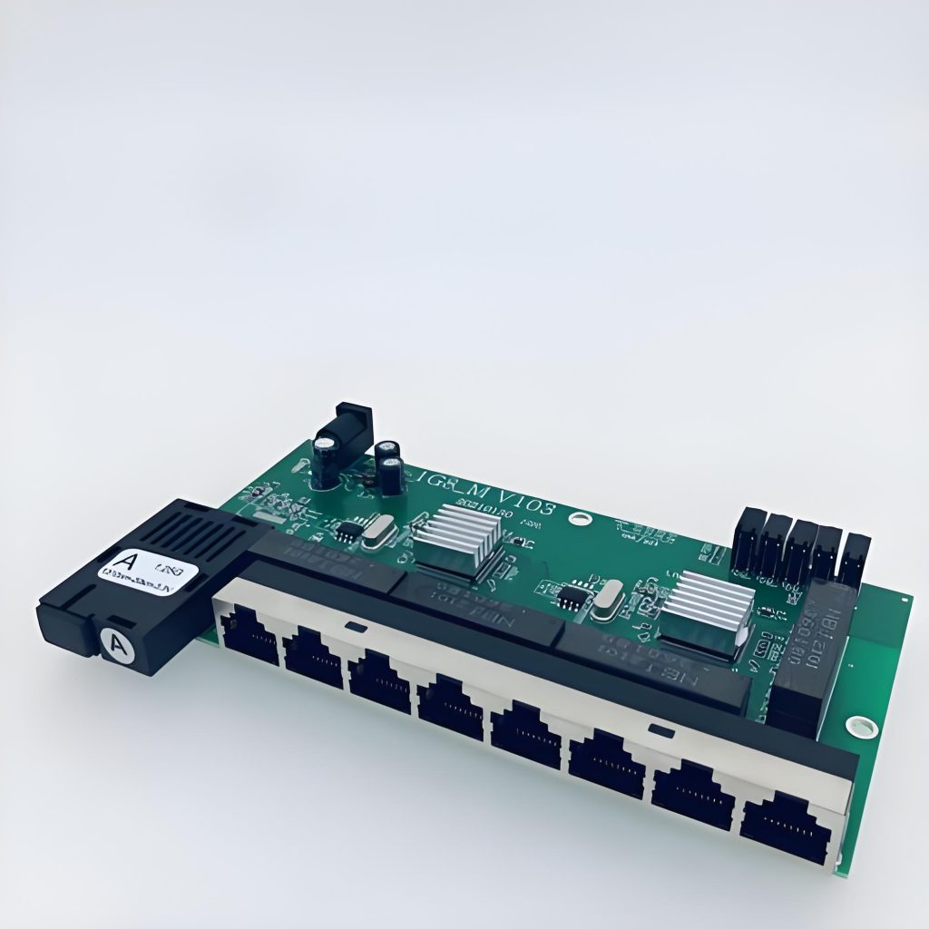
การควบคุมทางอุตสาหกรรม
- ตัวควบคุมตรรกะแบบโปรแกรมได้ของ PLC
- โมดูลการจัดการพลังงาน
- แผงวงจรเครื่องมือวัด
- บอร์ดควบคุมมอเตอร์ขับเคลื่อน
อุปกรณ์อิเล็กทรอนิกส์ยานยนต์ (ไม่มีความสำคัญต่อความปลอดภัย)
- ระบบสาระบันเทิงภายในรถยนต์
- โมดูลควบคุมตัวถัง
- บอร์ดอินเทอร์เฟซเซ็นเซอร์
การประกันคุณภาพและการปฏิบัติตามมาตรฐาน
มาตรฐานที่ใช้บังคับ
ผลิตภัณฑ์ PCB สารต้านอนุมูลอิสระ OSP ของ UGPCB ปฏิบัติตามมาตรฐานสากลเหล่านี้อย่างเคร่งครัด:
| มาตรฐาน | ชื่อ | ขอบเขต |
|---|---|---|
| ไอพีซี-4555 | ข้อกำหนดด้านประสิทธิภาพสำหรับสารกันบูดที่สามารถบัดกรีได้แบบอินทรีย์ที่อุณหภูมิสูง (โอป) สำหรับบอร์ดพิมพ์ลาย | ข้อกำหนดและการทดสอบกระบวนการ OSP |
| ไอพีซี-6012E | ข้อกำหนดคุณสมบัติและประสิทธิภาพสำหรับบอร์ดพิมพ์แข็ง | คุณภาพและประสิทธิภาพของบอร์ดสำเร็จรูป |
| IPC-4101/21 | ข้อกำหนดสำหรับลามิเนตอีพ็อกซี่เสริมกระจก | ข้อกำหนดทางเทคนิคของพื้นผิว FR-4 |
| IPC-TM-650 | คู่มือวิธีทดสอบ | วิธีทดสอบประสิทธิภาพต่างๆ |
| อล 94 วี-0 | ความไวไฟของวัสดุพลาสติก | ความปลอดภัยของสารหน่วงไฟของพื้นผิว |
| rohs 2.0 | การจำกัดการใช้สารอันตราย | การปฏิบัติตามข้อกำหนดด้านสิ่งแวดล้อม |
ตัวชี้วัดคุณภาพที่สำคัญ
ตามข้อกำหนด IPC, ตัวชี้วัดคุณภาพที่สำคัญ ได้แก่:
- ความหนาของฟิล์ม OSP: 0.2–0.5μm, ความทนทานต่อความสม่ำเสมอ ≤ ±0.1μm
- การยึดเกาะ: ≥4B (IPC-TM-650 2.4.29 การทดสอบแบบตัดขวาง)
- อัตราส่วนการแพร่กระจายของบัดกรี: ≥80% (IPC-TM-650 2.4.1)
- ระยะเวลาการป้องกันการเกิดออกซิเดชัน: ≥6เดือน (สภาพแวดล้อม)
- คะแนนความไวไฟ: อล 94 วี-0
เหตุใดจึงเลือก UGPCB สำหรับ PCB สารต้านอนุมูลอิสระ OSP?
ความสามารถในการผลิตที่แม่นยำ
- 0.15ความกว้างการติดตามขั้นต่ำ มม / 0.20ระยะห่างขั้นต่ำ มม
- 0.45มม. ขนาดรูสำเร็จรูปขั้นต่ำ
- 1.6ความหนาของแผ่นมาตรฐาน มม. พร้อมความเข้ากันได้ดีเยี่ยม
การควบคุมกระบวนการ OSP ที่เชื่อถือได้
- การปฏิบัติตาม IPC-4555 อย่างเข้มงวดสำหรับความหนาและคุณภาพของฟิล์ม
- สามารถตรวจสอบย้อนกลับได้อย่างสมบูรณ์ตลอดกระบวนการผลิต
- การทดสอบความสามารถในการบัดกรีและการสุ่มตัวอย่างความหนาของฟิล์มสำหรับทุกชุด
จัดส่งที่รวดเร็ว
- เวลานำมาตรฐาน: 7–10 วันทำการ
- รองรับทั้งการสุ่มตัวอย่างต้นแบบและการผลิตตามปริมาณ
การสนับสนุนทางเทคนิคที่ครอบคลุม
- รีวิวการออกแบบ DFM ฟรี
- ทีมวิศวกรมืออาชีพคอยให้คำแนะนำการเลือกผลิตภัณฑ์
รับใบเสนอราคาวันนี้เลย
UGPCB นำเสนอโซลูชันแผงวงจร PCB สารต้านอนุมูลอิสระ OSP ที่มีมูลค่าสูง. ไม่ว่าคุณจะต้องการการสุ่มตัวอย่างต้นแบบ หรือปริมาณการผลิต, เราให้การสนับสนุนด้านเทคนิคอย่างมืออาชีพและราคาที่แข่งขันได้.
📞 วิธีรับใบเสนอราคา:
- ส่งไฟล์ Gerber และรายการ BOM ของคุณ
- ทีมวิศวกรของเราตอบสนองด้วยโซลูชันที่กำหนดเองและเสนอราคาภายใน24 ชั่วโมง
- การตรวจสอบ DFM ฟรีเพื่อให้แน่ใจว่าการออกแบบของคุณผ่านในครั้งแรก
คำชี้แจงแหล่งข้อมูล: ข้อมูลทางเทคนิคและข้อกำหนดมาตรฐานที่อ้างถึงในเอกสารนี้มาจาก IPC เป็นหลัก (สมาคมเชื่อมต่ออุตสาหกรรมอิเล็กทรอนิกส์) มาตรฐานรวมถึง IPC-4555 “ข้อกำหนดด้านประสิทธิภาพสำหรับสารกันบูดที่สามารถบัดกรีได้แบบอินทรีย์ที่อุณหภูมิสูง (โอป) สำหรับบอร์ดพิมพ์ลาย,” ไอพีซี-6012E “ข้อกำหนดคุณสมบัติและประสิทธิภาพสำหรับบอร์ดพิมพ์แข็ง,” IPC-4101/21 “ข้อกำหนดสำหรับลามิเนตอีพ็อกซี่เสริมกระจก,” IPC-TM-650 “คู่มือวิธีทดสอบ,” และยูล 94 “มาตรฐานการทดสอบความไวไฟของวัสดุพลาสติกสำหรับชิ้นส่วนในอุปกรณ์และเครื่องใช้” พารามิเตอร์กระบวนการบางอย่างอ้างอิงข้อมูลทางเทคนิคที่เปิดเผยต่อสาธารณะจากผู้ผลิต PCB ชั้นนำ. ข้อมูลทั้งหมดได้รับการตรวจสอบความถูกต้องแล้ว.













