
ภาพรวมผลิตภัณฑ์: When Rigid Boards Learn to “Bend”
Modern electronic products demand smaller sizes and more features. Design engineers face a key challenge: fitting more circuit functions into limited space. Traditional rigid PCBS are flat and inflexible. Expensive flexible PCBs solve this but raise material costs and assembly complexity.
UGPCB introduces the Semi-Flex PCB (Semi-Flexible Printed Circuit Board) to solve this problem directly. It uses standard rigid FR-4 materials. Through precise controlled depth milling, specific areas of the board become bendable. This is not just a technical step forward. It is a cost revolution. You get the installation flexibility of rigid-flex boards at a cost closer to standard rigid boards.

What is a Semi-Flex PCB? More Than a One-Time Bend
A Semi-Flex PCB is also known as a “flex-to-install” board. It is not a traditional flexible circuit. แทน, it is a hybrid structure .
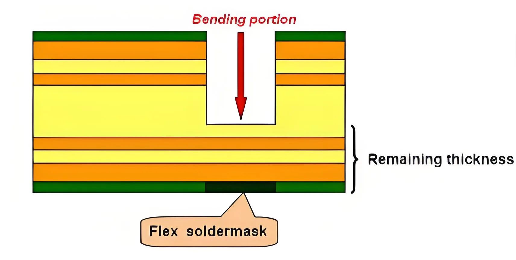
By definition, a Semi-Flex PCB starts as a standard rigid multilayer board. Using Controlled Depth Routing (CDR) , the FR-4 material in the bending area is thinned precisely. The remaining thickness is typically 0.2mm to 0.3mm. This thin section allows for limited, static bending. This bending usually happens only during installation, ซ่อมแซม, or rework. It is a “one-time bend” หรือ “flex-to-install” application.
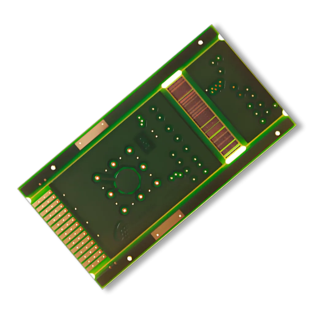
Core Parameters: UGPCB‘s Precision 8-Layer Solution
UGPCB designed this Semi-Flex PCB stack-up for demanding automotive electronics. Every data point ensures reliability.
| พารามิเตอร์ | ข้อมูลจำเพาะ | Technical Insight |
|---|---|---|
| จำนวนเลเยอร์ | 8l (15219) | A complex multilayer design for high-density wiring and strong signal integrity. |
| Bending Portion Conductive Layer | 2 ชั้น | Two copper layers within the thin 0.28mm bend area. This offers great routing freedom. |
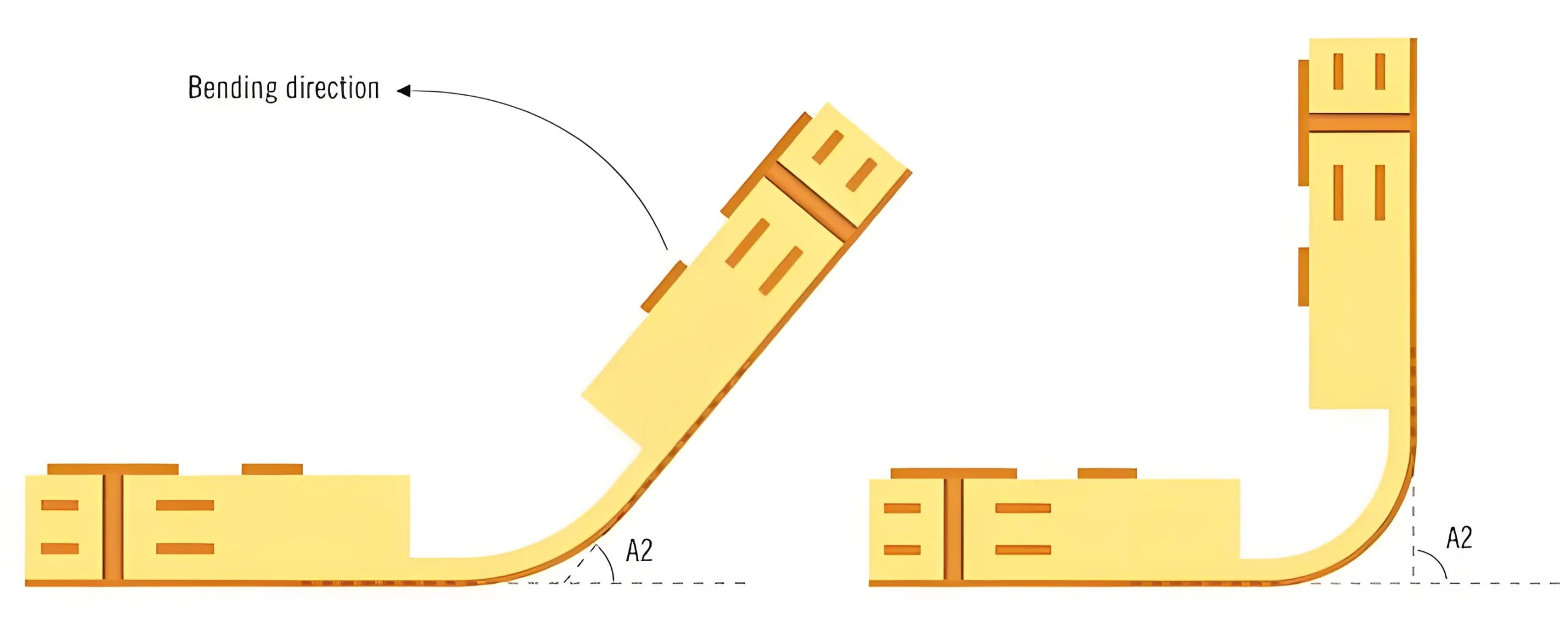
| Bending Angle | 180°, bi-directional | Supports extreme 180-degree folding in both directions. This offers excellent installation adaptability. |
| Remaining Thickness | สูงสุด: 0.28มม | Precise controlled depth milling achieves 0.28mm. This is a key value for reliable bending and strength. |
| Laminate Type | IT-158 | A high-Tg, high-reliability laminate ensures stability during lead-free soldering and high-temperature operation. |
| Bending Area PP Type | 1027 | Ultra-thin glass fabric prepreg. It ensures insulation and provides excellent bending flexibility. |
| Bending Area Solder Mask | PSR-9000 FLX501 | A special flexible solder mask. It replaces brittle standard ink and prevents cracking during bending. |
Design Essentials & หลักการทำงาน: The Art of Subtraction
หลักการทำงาน
The working principle of a Semi-Flex PCB is elegantly simple. It relies on physics. Controlled depth milling significantly reduces the FR-4 thickness in a specific area. When force is applied, this thinned FR-4 section deforms elastically, creating the bend .
Three Golden Design Rules
-
Controlled Depth Milling Accuracy: This is the core of Semi-Flex technology. The remaining thickness (like UGPCB‘s 0.28mm) must be precise. Too thick, and the board won’t bend or will crack. Too thin, and it loses mechanical strength. High-precision Z-axis controlled depth milling machines are required .
-
Bending Area Layout: The design must follow a “static bend” principle. The bend line should be perpendicular to the glass fiber weave direction for the best bend radius .
-
Stress Relief: Where the bend area meets the rigid area, traces must use rounded or teardrop shapes. Avoid 90-degree angles to prevent copper tearing during bending. Keep components at least 1mm away from the bend zone .
การใช้งาน & การจำแนกประเภท: Ideal for Static Bending
การจำแนกประเภททางวิทยาศาสตร์
-
โดยเทคโนโลยี: It belongs to 3D PCB การแก้ปัญหา. It serves as an economical alternative to traditional rigid-flex boards.
-
By Usage: It is a Static Flex PCB. This is different from dynamic flex boards designed for millions of flex cycles .
Main Applications
UGPCB Semi-Flex PCBs are ideal for these demanding environments:
-
อุปกรณ์อิเล็กทรอนิกส์ยานยนต์ (Customer Specified) : Ideal for instrument clusters, infotainment backplanes, and transmission control modules. The tight spaces inside vehicles benefit from Semi-Flex’s ability to fit irregular shapes .
-
การควบคุมอุตสาหกรรม: Used in robot I/O modules and inverters. It can replace cables and connectors, improving vibration resistance.
-
อุปกรณ์การแพทย์: Used in compact handheld devices and hearing aids. Its bending allows for very tight internal stacking.
ผลงาน, วัสดุ & โครงสร้าง: The Secret of Rigidity and Flexibility
Material Details
-
ลามิเนต (IT-158) : This is a high-heat-resistance FR-4. Its high glass transition temperature ensures stable dimensions and electrical performance after bending and during reflow soldering.
-
เตรียมการ (1027) : ที่ 1027 code indicates an extremely thin glass fabric. When laminated, it creates a very thin dielectric layer. This is key to achieving two copper layers within a total 0.28mm bend thickness .
-
Flexible Solder Mask (PSR-9000 FLX501) : Standard solder mask cracks like glass when bent. The FLX501 is a resin made for flexible circuits. It offers excellent elongation. It tightly wraps the circuits in the bend zone, preventing oxidation and shorts.
คุณสมบัติเชิงโครงสร้าง
A Semi-Flex PCB has two distinct zones: ที่ Rigid Area and the Bending Area.
-
Rigid Area: Maintains the standard 8-layer thickness (usually 1.6mm). This provides strong mechanical support for ส่วนประกอบ.
-
Bending Area: After controlled depth milling, only the thin core with two copper layers remains. The thickness is precisely controlled to 0.28mm. This asymmetrical structure demands advanced lamination and routing control.
กระบวนการผลิต: One Extra Step, Half the Cost
UGPCB follows a standardized Semi-Flex production flow. This ensures precise bending on every board.
-
การเคลือบ: Press IT-158 laminates, 1027 เตรียมการ, and high-ductility copper foil to form an 8-layer multilayer board .
-
การขุดเจาะ & การชุบ: Standard PCB processes create interlayer connections.
-
การถ่ายภาพชั้นนอก: Create the outer layer circuits. The bending area traces are already designed.
-
Flexible Solder Mask Application: Print PSR-9000 FLX501 flexible solder mask on the bending area [citation:provided_data]. Standard solder mask is not used here.
-
Controlled Depth Milling: Perform precision depth-controlled milling on the bending area. Reduce thickness to 0.28mm. This is the most critical step. Thickness tolerance must be within ±0.05mm .
-
Routing & การทดสอบ: Route the board outline. Conduct electrical tests to confirm circuits work after bending.
สถานการณ์การใช้งาน: Expanding Design Possibilities
-
Scenario 1: Replacing Expensive Cables: In a server backplane, a UGPCB Semi-Flex board can bend 90 degrees to connect directly. This saves the cost of FPC cables and connectors. It also reduces the risk of poor contact.
-
Scenario 2: LED Lighting: For circular or oddly shaped LED lamps, Semi-Flex can bend to the required curve. Its heat dissipation is much better than standard flexible PCBs.
-
Scenario 3: Security Cameras: Inside a PTZ camera dome, use Semi-Flex to connect the main board and the camera board as one unit. This saves space and improves vibration resistance.
Why Choose UGPCB Semi-Flex PCB?
-
Extreme Cost Control: Compared to traditional rigid-flex boards (using polyimide), Semi-Flex uses standard FR-4. Material costs drop by over 50%. Production cycles are also much shorter .
-
ความน่าเชื่อถือสูง: It avoids expensive flexible copper-clad laminates. This prevents delamination caused by CTE mismatch between flexible and rigid materials. This is vital for demanding fields like อุปกรณ์อิเล็กทรอนิกส์ยานยนต์ .
-
เสถียรภาพทางกล: With UGPCB‘s IT-158 laminates and 1027 เตรียมการ, the board maintains its shape after 180-degree bi-directional bending. Spring-back is minimal.
-
High Customization: Whether 4-layer or 8-layer, single-layer or double-layer copper in the bend area (like the 15219 stack-up), UGPCB provides one-stop service from engineering samples to mass production.
Get a Quote Now. Unlock Your 3D Design Potential.
Semi-Flex PCB technology is changing how engineers design products. It lets you prioritize circuit performance and layout without being limited by space.
Don’t let connectors and cables restrict your designs.
UGPCB has mature experience in Semi-Flex mass production. 8-บอร์ดเลเยอร์, 180-degree bending, 0.28mm remaining thickness… We don’t just build your design. We ensure long-term reliability.
[Click Here to Get a Free Engineering Review & Quote from UGPCB] (คำกระตุ้นการตัดสินใจ)


