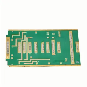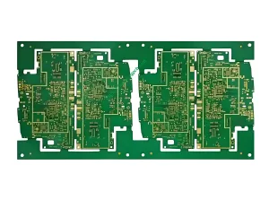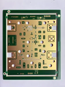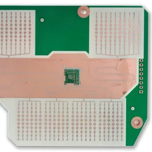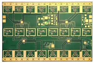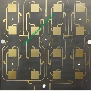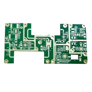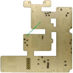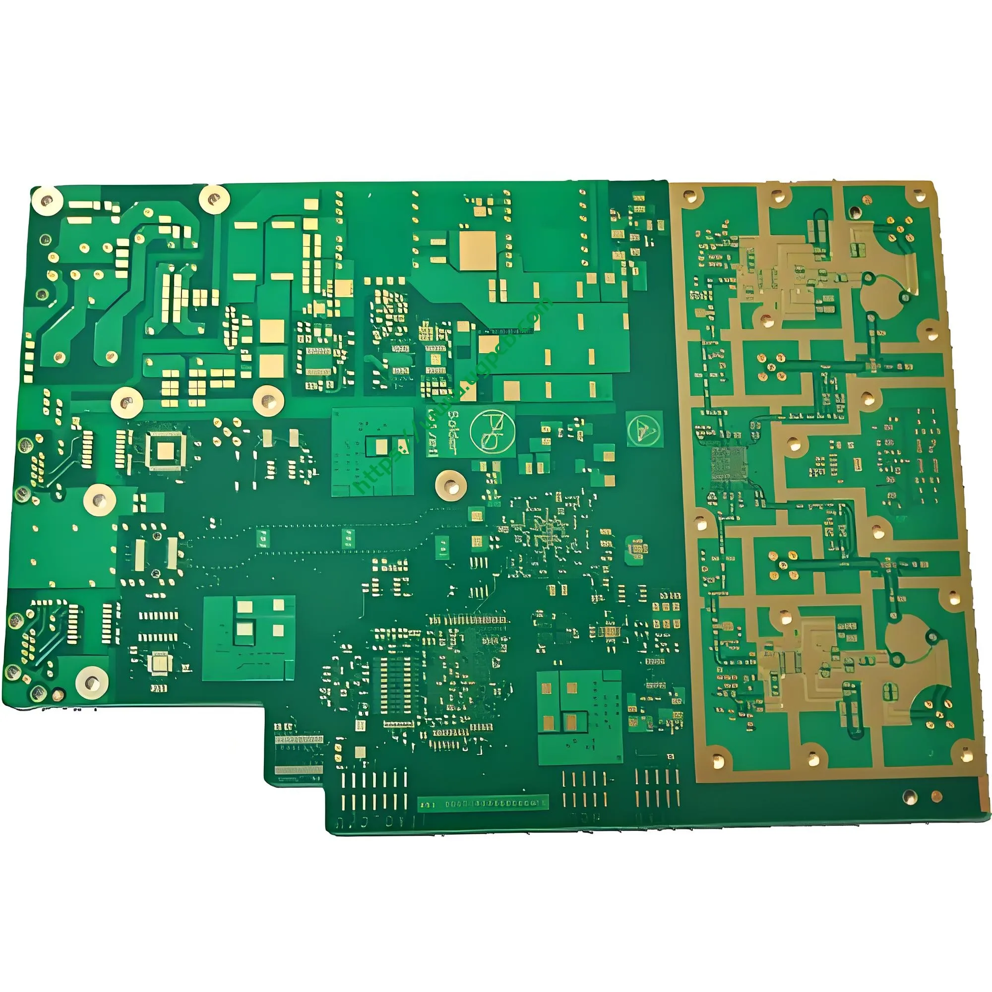
A medida que las interfaces de RF y los circuitos digitales de alta velocidad continúan convergiendo, Los ingenieros de diseño de PCB se enfrentan a un dilema clásico. un puro FR4 La placa sufre una pérdida excesiva de señal y una mala control de impedancia en altas frecuencias. Una solución Rogers de pensión completa ofrece un excelente rendimiento de RF, pero cuesta mucho más y limita la capacidad de fabricación. El 6-placa híbrida de alta frecuencia de capa resuelve este compromiso con un diseño dieléctrico mixto inteligente.
1. Producto Descripción general
UGPCB 6-PCB híbrido de alta frecuencia de capa usos Rogers RO4350B y FR4 materiales en una pila mixta. El acabado superficial es Oro de inmersión (ACEPTAR). Este tablero apunta ETC (Cobro electrónico de peaje) tableros de control del sistema y otras aplicaciones de RF de 5,8 GHz. Se logra precisión 5/4 Ancho de traza MIL y espaciado para enrutamiento de RF de alta densidad. A 5-6 capa ciega vía La estructura optimiza las rutas de señal..
2. ¿Qué es una PCB híbrida de alta frecuencia??
Una PCB híbrida de alta frecuencia, También llamado tablero multicapa de dieléctrico mixto., combina dos o más materiales de sustrato diferentes en una sola placa. Las capas de alta frecuencia utilizan material Rogers de baja pérdida. (como RO4350B). Las capas no críticas y las capas digitales/de energía utilizan FR4 más económico..
Este enfoque híbrido coloca material de primera calidad solo donde el rendimiento de RF importa, por ejemplo, en la capa superior donde la guía de ondas microstrip o coplanar transporta señales de 5,8 GHz. Las otras capas de señal, planos de tierra, y las capas de energía usan FR4. Comparado con una tabla Rogers completa, El diseño híbrido reduce el coste del material en 40–60% manteniendo casi el mismo rendimiento de RF.
3. Parámetros técnicos clave
| Parámetro | Especificación |
|---|---|
| Número de capas | 6 |
| Materiales mixtos | Rogers RO4350B + FR4 |
| Acabado superficial | Oro de inmersión (DE ACUERDO según IPC-4552A, De 3 a 6 μm / Au 0,04–0,1 μm) |
| Característica del producto | Placa híbrida de alta frecuencia |
| Solicitud | Tablero de control del sistema ETC |
| Proceso especial | Vías ciegas entre capas 5 y 6 |
| Ancho de traza / espaciado | 5/4 MIL |
| Relación de espesor del agujero al tablero | 1:10 |
4. Propiedades del material de alta frecuencia Rogers RO4350B
El rendimiento de RF de esta placa híbrida depende del uso preciso de Rogers RO4350B. Características eléctricas y térmicas clave. (fuente: Ficha técnica de Rogers Corporation, probado según IPC-TM-650) se enumeran a continuación.
-
Constante dieléctrica (Dk): 3.48 ±0,05 @ 10 GHz (referencia del proceso); 3.66 @ 10 GHz (referencia de diseño para espesor >60mil)
-
factor de disipación (df): 0.0037 @ 10 GHz
-
CTE del eje z (coeficiente de expansión térmica): 32 ppm/°C (–55°C a 288°C) – mucho mejor que el FR4 estándar, lo que reduce el riesgo de agrietamiento
-
Conductividad térmica: 0.69 W/m/°K a 50°C (Norma ASTM D5470)
-
Clasificación de inflamabilidad: UL 94 V-0 – cumple con los requisitos de seguridad para dispositivos activos y diseños de RF de alta potencia
-
Compatibilidad de procesos: No se necesita preparación especial vía (a diferencia de los materiales de PTFE); RO4350B procesa de manera similar a FR4, lo que reduce el costo de producción
Por qué esto importa: El Dk del RO4350B cambia muy poco de 500MHz a 40GHz. Esta estabilidad permite a los ingenieros diseñar líneas de transmisión de impedancia precisas de 50 Ω o 75 Ω en un amplio ancho de banda.. Para sistemas ETC que funcionan a 5,8 GHz (para GB/T 20851), esto significa control de impedancia confiable. Por ejemplo, utilizando una estructura de microcinta con Dk=3,48, espesor del tablero = 0.254 mm, y 1oz de cobre, un ancho de traza de 5 mil logra una impedancia característica de 50 Ω según la siguiente fórmula.
5. ¿Cómo funciona una placa híbrida de alta frecuencia de 6 capas??
El principio básico es una arquitectura de señal dedicada a capas..
-
Capas de señal de RF (Rogers RO4350B mediano) – Ubicado en la capa superior o capas internas específicas. Llevan señales de comunicación ETC de 5,8GHz.. El Dk estable y el bajo Df del RO4350B mantienen la pérdida de inserción por debajo de 0,31 dB/cm a 40 GHz..
-
Capas digitales/de control (FR4 medio) – Manejar señales de banda base, Control lógico MCU/FPGA, y gestión de energía. FR4 aporta bajo costo y buena resistencia mecánica.
-
Tierra de referencia y capas de energía. – Un plano de tierra sólido adyacente a las capas de RF proporciona una ruta de retorno de baja impedancia y suprime la EMI.
-
5-Vías ciegas de 6 capas – Las vías ciegas conectan solo capas específicas (p.ej., L5 a L6). Reducen la capacitancia y la inductancia parásitas en comparación con las vías de orificio pasante., y ahorran espacio de enrutamiento.
-
Diseño con impedancia adaptada – Utilizando el valor Dk preciso de RO4350B, la impedancia controlada (normalmente 50Ω) se calcula con la fórmula de microstrip:
 Dónde:
-
εr=3,48 (RO4350B Negro)
-
H = grosor dieléctrico (mils)
-
w = Ancho de rastreo (5 mils)
-
t= grosor de cobre (mils)
Esta fórmula, combinado con simulaciones de resolución de campo, garantiza un control preciso de 50 Ω.
6. Aplicaciones y casos de uso
La aplicación principal de esta PCB híbrida de 6 capas es la placa de control del sistema ETC.. También se adapta a muchos otros DSRC de 5,8 GHz. (comunicación dedicada de corto alcance) dispositivos.
-
Unidad de carretera ETC (RSU) tablero de control – Transceptor frontal de RF + procesamiento de banda base + gestión de energía. ETC sigue el estándar nacional chino GB/T 20851 a 5,8 GHz utilizando modulación ASK y protocolo DSRC.
-
Unidad a bordo ETC (OBU) tablero principal – También funciona a 5,8 GHz, con circuito de activación de potencia ultrabaja de 5 µA y transceptor de RF integrado.
-
5Módulos frontales de estación base G – Integración mixta de procesamiento de señales de microondas y control de banda base digital..
-
Radar de ondas milimétricas para automóviles (24GHz / 77GHz) – RO4350B funciona de forma fiable hasta 40 GHz, Cumplir con los requisitos de los radares automotrices en cuanto a ruido de fase y estabilidad de temperatura..
-
Wi‑Fi 6/7 enrutadores – Tarjeta mixta para enlaces de datos de alta velocidad de 5 a 7 GHz con front-end RF y SoC digital.
-
Módulos de comunicación por satélite. – Integración híbrida de bajo costo de recepción de alta frecuencia y demodulación digital.

7. Clasificación de productos
Por IPC-6018D (Especificación de calificación y rendimiento para alta frecuencia (Microonda) Tableros impresos), este producto cae en las siguientes categorías.
-
clase principal: Tablero impreso para microondas de alta frecuencia
-
Subclase: Multicapa dieléctrica mixta: un tablero que combina dos o más materiales de sustrato con diferentes valores Dk en una pila
-
Clase de característica: Multicapa con vías ciegas: verificado mediante los métodos de prueba IPC‑6018D
-
Conformidad de materiales: Los materiales base cumplen con IPC‑4101E (Especificación de Materiales Base para Tableros Impresos Rígidos y Multicapa) para rendimiento de alta frecuencia/alta velocidad
8. Directrices de diseño para placas híbridas de alta frecuencia
Los ingenieros de diseño deben centrarse en estas cinco áreas críticas.
-
Apilamiento y asignación de materiales – Decide qué capas obtienen Rogers y cuáles obtienen FR4. También define el orden de las capas. (señal de radiofrecuencia, suelo, señal digital, fuerza). Controle estrictamente el espesor de cada capa para garantizar la precisión de la impedancia.
-
Coincidencia de impedancia – El control preciso de 50 Ω es el corazón del diseño de PCB de alta frecuencia. La tolerancia Dk de RO4350B (±0,05) afecta directamente al error de impedancia. Ejecute siempre simulaciones de resolución de campo 2D o 3D para verificar la continuidad de la impedancia y la integridad de la señal..
-
Ciego mediante optimización (capas 5–6) – Las vías ciegas conectan solo capas específicas (p.ej., L5 a L6). Reducen la capacitancia parásita. cs e inductancia parásita ls en comparación con a través de vías. Minimice la cantidad de vías ciegas en rutas de señales de alta frecuencia y optimice la ubicación de las vías para evitar discontinuidades de impedancia..
-
Emparejamiento CTE y laminación híbrida. – RO4350B tiene un CTE que coincide bien con el cobre (10–12 ppm/°C en ejes X/Y). Sin embargo, FR4 y Rogers se comportan de manera diferente durante el ciclo térmico. Utilice laminación gradual con una curva de presión dinámica para evitar la delaminación.
-
Integridad de la señal (Y) análisis – Simular la pérdida de inserción, diafonía, reflexión, y margen de sincronización a 5,8 GHz. Verifique que el enlace funcione por debajo de la tasa de error de bits objetivo.
9. Proceso de fabricación
UGPCB sigue un estricto proceso de 8 pasos para garantizar que cada placa híbrida de 6 capas cumpla con los más altos estándares de calidad..
-
coeficiente intelectual (control de calidad entrante) – Inspeccionar las materias primas según IPC‑4101E y la tolerancia Dk de Rogers. (±0,05).
-
Imágenes de la capa interna – Usar LDI (Imágenes directas láser) para lograr 5/4 Ancho y espaciado de traza MIL.
-
Óxido y estratificación – Alinee las capas RO4350B y FR4 con precisión.
-
Laminación híbrida – Aplique un perfil de temperatura gradual y una curva de presión dinámica para curar ambos materiales juntos, evitando la delaminación y la deformación.
-
Perforación - taladro láser Vías ciegas para las capas 5 a 6 y, opcionalmente, utilizar perforación trasera.. Mantener el 1:10 Relación de espesor del agujero al tablero dentro de la tolerancia.
-
desmechar, cobre no electrolítico, y revestimiento de paneles – Garantice una cobertura de cobre confiable en paredes de vía ciega según la clase IPC‑6018D 3.
-
Imagen de capa exterior y revestimiento de patrón. – Crea finos trazos exteriores y resiste el grabado..
-
Máscara de soldadura y leyenda. – Aplicar máscara de soldadura e imprimir identificadores de componentes..
-
ACEPTAR (Oro de inmersión) acabado superficial - Deposito Ni (3–6 μm) y au (0.04-0,1 µm) según IPC‑4552 A/B.
-
Enrutamiento y puntuación V – Ruta hacia la forma final y puntuación V para la despanelización.
-
prueba electrica - Usar sonda voladora para verificar la continuidad y el aislamiento.
-
FQC e inspección de salida – Dimensiones de verificación de muestras y rendimiento de RF. Todos los productos cumplen con los estándares de calidad de las placas híbridas..
10. Certificaciones y estándares de calidad
Las placas híbridas de alta frecuencia de 6 capas de UGPCB cumplen totalmente con los siguientes estándares de la industria.
-
IPC-6018D – Calificación y rendimiento para alta frecuencia. (microonda) tableros impresos, que cubren multicapas de dieléctrico mixto y vías ciegas/enterradas.
-
IPC-4101E – Especificación de materiales base para tableros impresos rígidos y multicapa, asegurando electricidad, térmico, y rendimiento mecánico.
-
IPC‑4552A/B – especificación ENIG, Garantizar el espesor y la uniformidad del níquel y el oro para soldar y unir cables..
-
UL 94 V‑0 – Clasificación de inflamabilidad para dispositivos activos y diseños de RF de alta potencia.
-
IPC‑TM‑650 – Manual de métodos de prueba., utilizado para medir Dk, df, y otros parámetros críticos del RO4350B.
11. Por qué elegir UGPCB para su placa híbrida de alta frecuencia de 6 capas?
-
Rendimiento superior de alta frecuencia – El Dk estable del RO4350B permite una adaptación precisa de la impedancia con 5/4 Trazas MIL y baja pérdida de inserción. La calidad de la señal de RF coincide con las placas de microondas de alta gama..
-
Importantes ahorros de costes – Diseño híbrido (Rogers solo en capas de RF, FR4 en otros lugares) Reduce los costos de material y fabricación entre un 40% y un 60% en comparación con una tabla Rogers completa..
-
Optimizado para sistemas ETC – La placa está sintonizada para comunicación DSRC de 5,8 GHz y sigue China GB/T 20851 estándares.
-
Capacidad de fabricación avanzada – Soportes 5/4 Líneas finas MIL, 1:10 relación de espesor del agujero al tablero, y vías ciegas de 5 a 6 capas: ideales para diseños de RF de alta densidad tipo HDI.
-
Proceso compatible con IPC – Control total del proceso IPC desde IQC hasta FQC, certificado según IPC‑6018D para multicapas dieléctricas mixtas.
-
Servicio integral – Desde la revisión del diseño y los prototipos hasta la producción en volumen.. Nuestros ingenieros experimentados en PCB de RF lo apoyan en cada etapa.
12. Obtenga una cotización o comience su pedido
UGPCB tiene años de experiencia en la fabricación de placas híbridas de alta frecuencia. Hemos entregado muchos PCB híbridos Rogers+FR4 de 6 capas para sistemas ETC, 5comunicación g, y radar automotriz.
Proceso de pedido:
-
Envía tus archivos de diseño – Gerber, dibujo apilado, lista de materiales, y requisitos técnicos.
-
Revisión técnica – Los ingenieros de UGPCB responden dentro 24 horas con informe DFM y cotización.
-
Confirmar pedido – Firmar el contrato y pagar el depósito..
-
Producción – IQC → control en proceso → FQC → pruebas de rendimiento.
-
Entrega – Recibir tablero con informe de inspección saliente., certificados de materiales, e informe de prueba eléctrica.
📧 Correo electrónico: ventas@ugpcb.com
📞 Teléfono: +86 135 4412 8719
🌐 Sitio web: https://www.ugpcb.com/