Introducción a la 6 PCB de capa
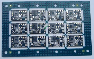
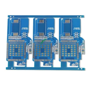
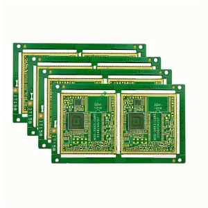
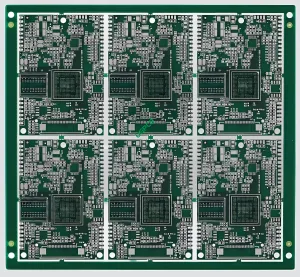
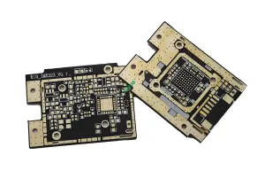
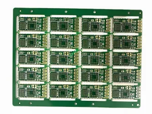
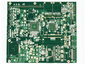
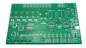
El 6 Layer PCB es un sofisticado componente electrónico Diseñado para aplicaciones de alto rendimiento que requieren circuitos complejos.. Consta de seis capas de material conductor., típicamente cobre, separados por capas aislantes. Esta estructura multicapa permite una mayor funcionalidad y compacidad en comparación con una sola o PCB de doble cara.
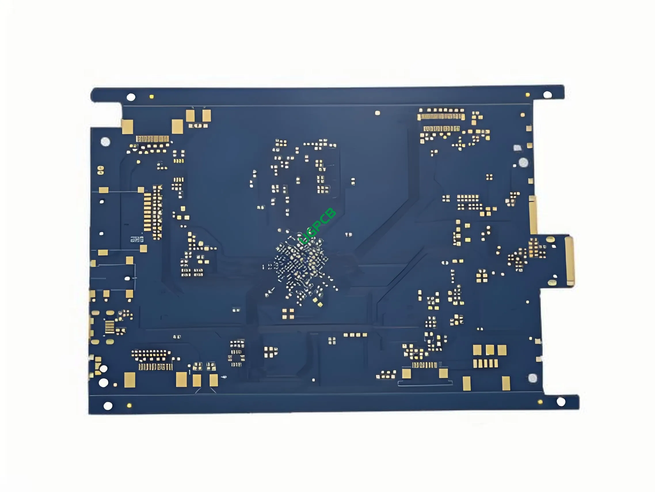
¿Qué es un 6 PCB de capa?
A 6 PCB de capa, o Placa de circuito impreso, es un sustrato electrónico avanzado que presenta seis capas de vías conductoras incrustadas dentro de capas aislantes. Estas capas están meticulosamente dispuestas para crear diseños de circuitos complejos adecuados para aplicaciones electrónicas exigentes.. Las capas adicionales proporcionan una integridad de señal mejorada, distribución de energía, y capacidades de gestión térmica.
Requisitos de diseño
Diseñando un 6 La PCB en capas implica varias consideraciones críticas:
- Selección de material: Los materiales comunes incluyen S1141, S1000, y 370HORA, elegidos en función de sus propiedades eléctricas y compatibilidad con el proceso de fabricación.
- Apilamiento de capas: Determina la disposición de los planos de señal y tierra., crucial para minimizar la diafonía y garantizar una transmisión de señal confiable.
- Espesor de cobre: Normalmente se especifica como 1/H/H/H/H1 OZ, indicando diferentes espesores en diferentes capas para optimizar el rendimiento y el costo.
- Tratamiento superficial: Opciones como Immersion Gold u OSP (Protección de organosilicio) Se aplican para proteger las superficies de cobre y mejorar la soldabilidad..
¿Cómo funciona??
El 6 La PCB en capas funciona proporcionando una plataforma para que los componentes eléctricos se interconecten a través de una serie de caminos conductores grabados en su superficie.. Cada capa contiene patrones específicos de trazas de cobre que forman circuitos cuando se conectan a través de orificios pasantes o vías enchapadas.. Las múltiples capas permiten diseños de circuitos más complejos sin aumentar el tamaño de la placa., haciéndolo ideal para dispositivos electrónicos modernos donde el espacio es limitado.
Aplicaciones
Debido a su complejidad y capacidad para manejar señales de alta velocidad con mínima interferencia, 6 Los PCB en capas se utilizan ampliamente en la electrónica de consumo, como los teléfonos inteligentes., tabletas, computadoras portátiles, y otros dispositivos portátiles. También se encuentran en la electrónica del automóvil., equipo medico, y controles industriales donde la confiabilidad y el rendimiento son primordiales.

Clasificación
6 Los PCB en capas se pueden clasificar en función de varios factores:
- Por material: Como se mencionó, pueden usar S1141, S1000, o 370HR dependiendo de las características requeridas.
- Por aplicación: De uso general o especializado para industrias específicas como las telecomunicaciones., aeroespacial, o defensa.
- Por tratamiento superficial: Diferentes acabados como Immersion Gold u OSP se adaptan a diversas condiciones ambientales y procesos de soldadura..
Materiales utilizados
Los materiales primarios utilizados en la fabricación. 6 Los PCB de capa incluyen:
- Materia prima: A menudo, resinas epoxi reforzadas con fibra de vidrio. (FR-4), que ofrecen una excelente resistencia mecánica y estabilidad térmica..
- Lámina de cobre: Se utilizan diferentes espesores para equilibrar la conductividad y la rentabilidad..
- Máscara de soldadura: Generalmente de color verde, protege las trazas de cobre de la oxidación y de cortocircuitos accidentales.
- Serigrafía: Una capa blanca que se utiliza para etiquetar componentes y proporcionar instrucciones de montaje..
Características de rendimiento
Atributos clave de rendimiento de un 6 PCB de capa incluye:
- Integridad de señal: Mejorado por la colocación estratégica de capas y esquemas de puesta a tierra..
- Gestión Térmica: Disipación de calor mejorada debido a áreas de cobre más grandes y tableros potencialmente más gruesos.
- Resistencia mecánica: La construcción multicapa añade rigidez, Reducir el riesgo de daños durante la manipulación u operación..
Composición estructural
Estructuralmente, a 6 PCB de capa comprende:
- Capas conductoras: Seis capas de trazas de cobre separadas por materiales dieléctricos..
- Capas aislantes: Evite cortocircuitos eléctricos entre capas conductoras.
- Vías: Agujeros conductores que conectan diferentes capas., permitiendo la integración vertical de circuitos.
Características distintivas
Algunas características notables de un 6 PCB de capa son:
- Densidad alta: Permite diseños de circuitos complejos dentro de un factor de forma compacto.
- Fiabilidad: El diseño multicapa mejora la resistencia a las interferencias electromagnéticas (EMI).
- Versatilidad: Adecuado para una amplia gama de aplicaciones gracias a las configuraciones de capas personalizables y a la elección de materiales.
Proceso de producción
El proceso de fabricación de un 6 PCB en capas implica varios pasos:
- Diseño y diseño: Usar software especializado para crear el patrón del circuito..
- Preparación de material: Cortar materiales base a medida y limpiar superficies..
- Laminación: Apilar y unir capas individuales bajo calor y presión..
- Aguafuerte: Eliminar el exceso de cobre para formar las rutas de circuito deseadas..
- Enchapado: Agregar una fina capa de metal a las vías y áreas de cobre expuestas.
- Aplicación de máscara de soldadura: Aplicar la capa verde para proteger los rastros..
- Serigrafía: Agregar texto y símbolos para la ubicación de componentes.
- Inspección final: Garantizar la calidad y la funcionalidad antes del envío.
Casos de uso
Escenarios comunes donde un 6 Se podrían emplear PCB en capas, entre ellas::
- Aplicaciones de interconexión de alta densidad en dispositivos móviles.
- Sistemas de comunicación avanzados que requieren baja pérdida de señal.
- Instrumentos médicos portátiles que necesitan un rendimiento confiable en entornos hostiles.
- Electrónica automotriz que exige robustez y longevidad.
En resumen, el 6 Layer PCB representa un avance significativo en la tecnología de placas de circuito impreso, Ofrece complejidad y rendimiento incomparables para aplicaciones electrónicas modernas.. Su flexibilidad de diseño., combinado con una integridad y durabilidad de señal superiores, lo convierte en un componente esencial en el desarrollo de la electrónica de consumo de próxima generación y más allá.