
RO4350B Hybrid Lamination High-Frequency PCBs: The Optimal Solution for 5G and RF Applications
|Facing the high-frequency design dilemma of performance versus cost, an engineer at a communications equipment manufacturer reduced antenna module loss by 40% while staying within budget by adopting a hybrid lamination strategy.
With the rapid advancement of 5G, radar automotriz, and other high-frequency applications, signal stability and integrity are now critical determinants of electronic device performance.
UGPCB’s RO4350B Hybrid High-Frequency PCBs utilize a unique construction that laminates Rogers RO4350B high-frequency material with standard FR-4. This approach delivers superior RF performance while maximizing cost efficiency, providing an ideal solution for demanding high-frequency circuits.
01 Product Core: Definición & Unique Value
The RO4350B Hybrid PCB is an innovative composite structure. Its core innovation is the precise lamination of high-performance Rogers RO4350B material with cost-effective FR-4 within a single board.
This design is strategic. The fundamental principle is optimal material distribution based on circuit function.
-
RO4350B is used for RF circuits, antenna feedlines, and other areas demanding utmost signal integrity.
-
FR-4 is used for power management, digital control, and other low-frequency sections.
The direct advantage is significantly enhanced system integration. Designers can integrate RF front-end modules (p.ej., PAs, LNAs) with digital control circuits on the same board. This reduces connectors, saves space, and improves overall reliability by eliminating inter-board interconnects.
02 Material Analysis: RO4350B & FR-4 Synergy
Understanding this product’s benefit requires examining both core materials.
Rogers RO4350B is a ceramic-filled hydrocarbon/glass laminate designed for RF. Its most prominent feature is a stable, controlled Constante dieléctrica (Dk) de 3.48 ±0,05, ensuring consistent electrical performance across batches and board locations. This is crucial for precise impedance control. Es Factor de disipación (df) is a low 0.0037 @ 10 GHz, minimizing high-frequency signal loss. Unlike traditional PTFE materials, RO4350B can be processed using standard FR-4 protocols, reducing manufacturing cost and complexity.
FR-4, in contrast, is the universal, economical workhorse of the tarjeta de circuito impreso industria. It offers unmatched mechanical strength, multi-layer processing maturity, y bajo costo, but suffers from higher loss and less stable Dk at high frequencies.
The ingenuity of the RO4350B hybrid PCB lies in leveraging each material’s strengths, striking the optimal engineering balance between performance and cost.
03 Actuación: Key Parameters & Design Essentials
The performance is defined by material properties and precise design. These key parameters are critical:
-
Constante dieléctrica estable (Dk): RO4350B’s Dk is 3.48 @ 10 GHz with a tight tolerance of ±0,05. Its thermal coefficient of Dk is typically +50 ppm/°C de -50°C to +150°C, ensuring stable performance across operating environments.
-
Baja pérdida: The low Df translates directly to lower signal attenuation. This is vital for efficiency and range in 5G (up to 28GHz) and automotive radar applications.
-
Superior Thermal Management: With a thermal conductivity of 0.69 W/m/K, it aids component cooling. Its low Z-axis CTE (32 ppm/°C) closely matches copper, reducing the risk of via cracking during thermal cycling.
-
Alta fiabilidad: The material is UL 94 V-0 calificado, suitable for active and high-power designs.
-
Precise Impedance Control: The hybrid structure requires complex impedance modeling. Expert manufacturers like UGPCB achieve high-standard control, como ± 8% or better, through deep process know-how.
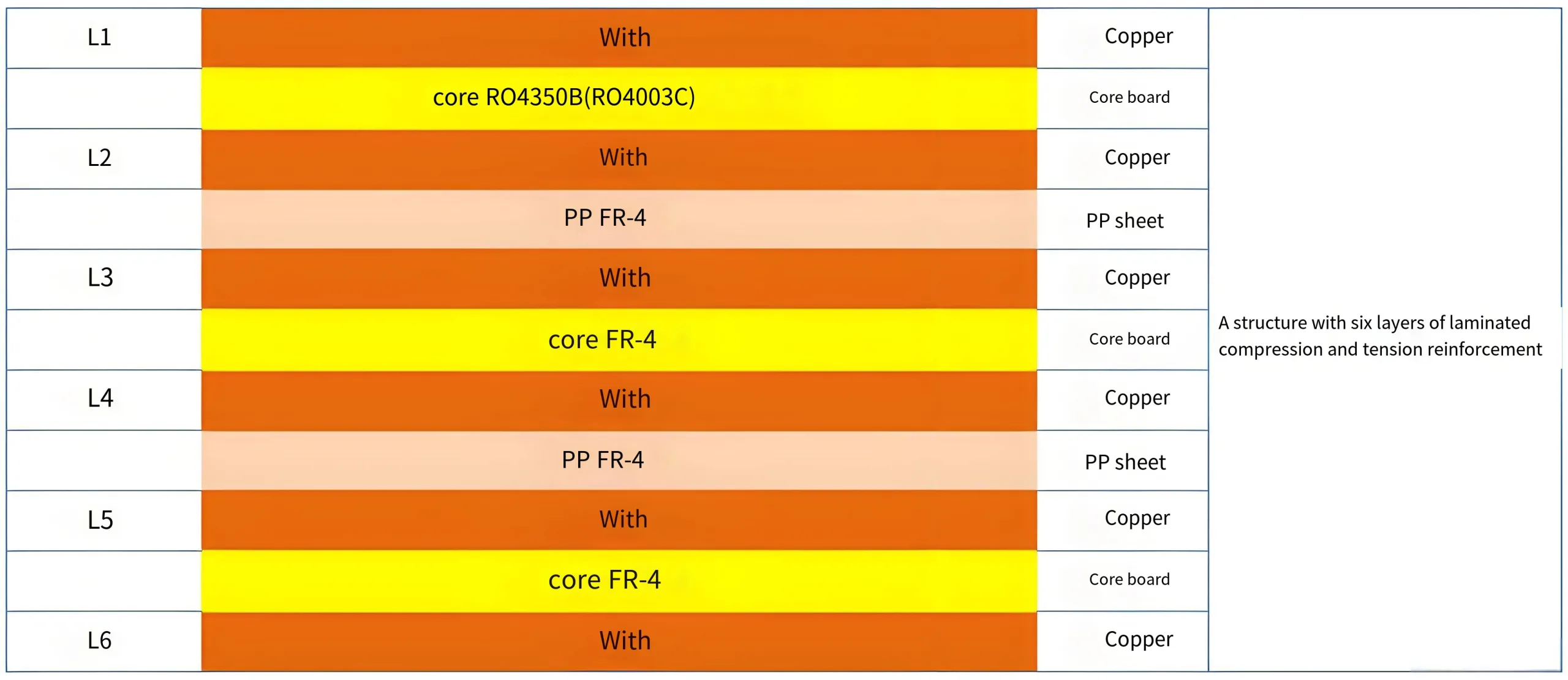
04 Fabricación de precisión: Hybrid Lamination Process
Producing these PCBs tests a manufacturer’s technical capability, centering on reliably bonding two dissimilar materials.
The process starts with precise material prep and inner-layer processing of separate RO4350B and FR-4 cores. Drilling parameters are adjusted for the more brittle RO4350B.
The critical Multi-Layer Lamination stage stacks the different cores and prepreg (PÁGINAS). The challenge is balancing the materials’ different CTEs and flow properties. Optimized lamination profiles (temperatura, pressure curves) are essential to ensure bond strength and prevent delamination or blistering.
Post-lamination, the panel undergoes drilling, enchapado, outer-layer imaging, máscara de soldadura, and surface finish. ACEPTAR is commonly used for its flat surface, good solderability, and stable contact resistance, ideal for RF connections.
Rígido Control de calidad throughout, including impedance coupon monitoring, AOI, and electrical testing, ensures every board meets specifications.
(Imagen: Flowchart of the hybrid PCB manufacturing process from material prep to final test. ALT: RO4350B hybrid PCB manufacturing process flowchart showing lamination and testing steps.)
05 Aplicaciones: From 5G to Autonomous Driving
RO4350B Hybrid PCBs are key enablers in several cutting-edge fields:
-
5G Infrastructure: Ideal for Active Antenna Units (AAU). Antenna elements are placed on RO4350B for optimal radiation, while feed networks and control circuits integrate on FR-4, achieving high integration at controlled cost.
-
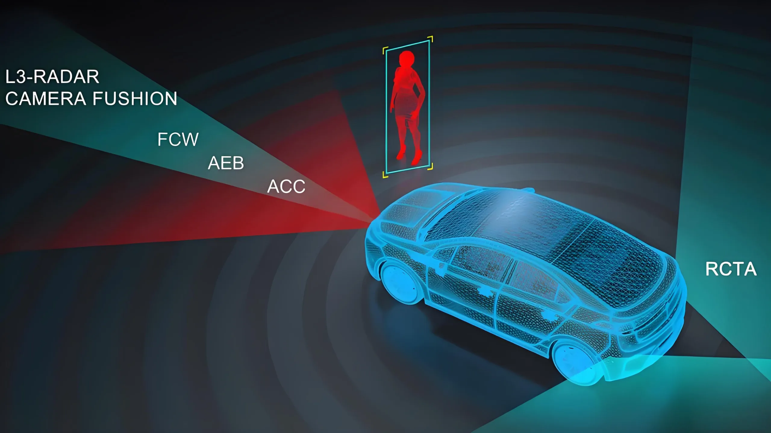
Electrónica automotriz: Critical for 77GHz radar sensors. Stable RF performance ensures detection accuracy, while thermal and mechanical reliability suits harsh under-hood environments.
-
RFID & Satellite Comms: Low loss improves sensitivity in devices like LNBs.
-
Other Key Uses: High-end instrumentation, point-to-point radio links, and RF front-end modules for Wi-Fi 6/7 enrutadores, enabling high-performance, miniaturized designs.
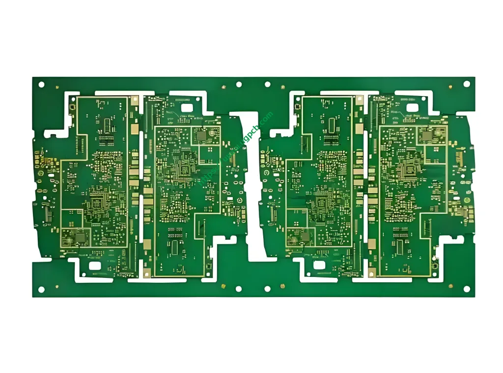
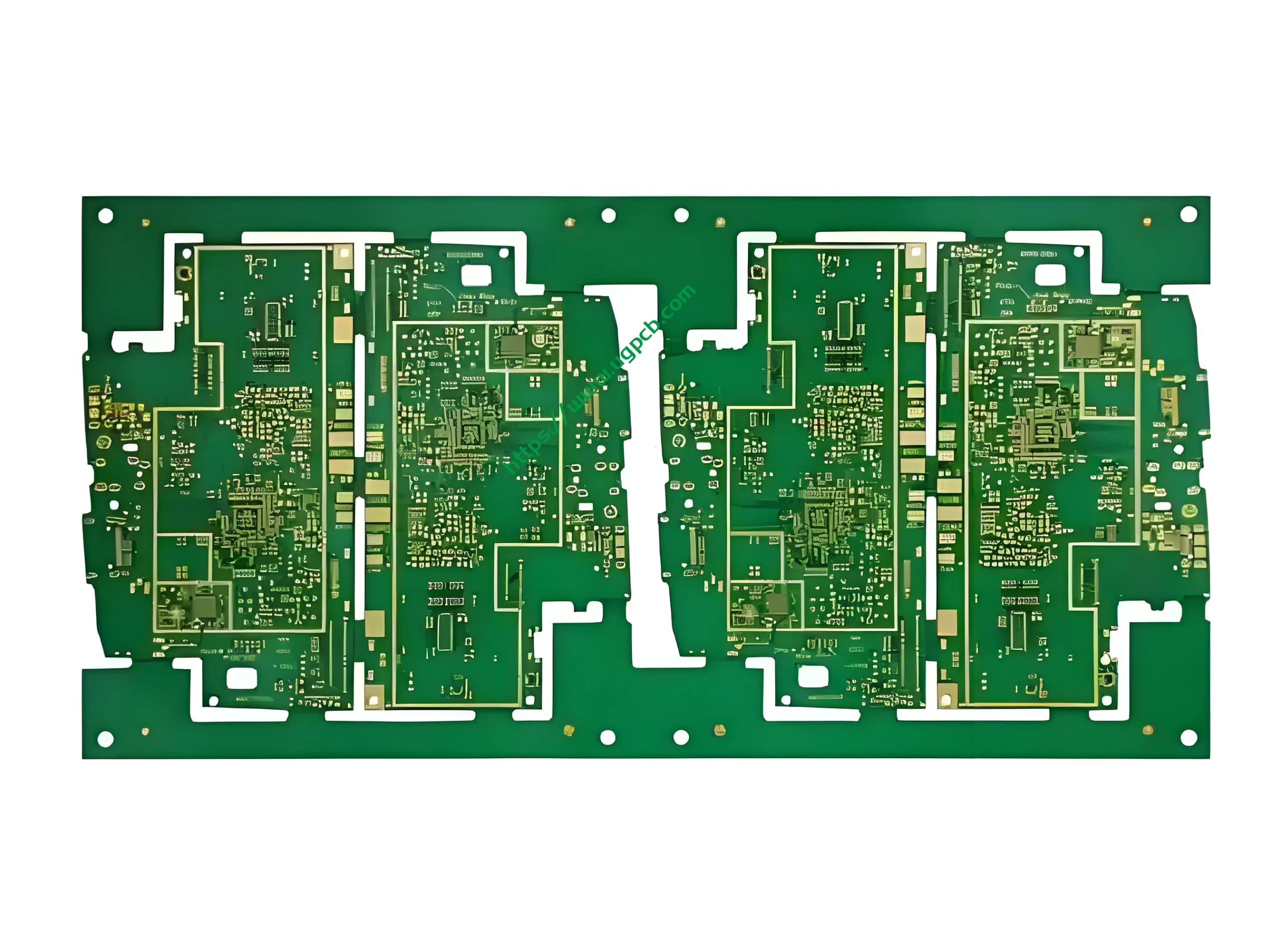
On the board, a clear boundary exists: one side is the darker Rogers RO4350B area with delicate microwave circuits; the other is the standard FR-4 region, populated with power and digital chips. This invisible line defines the perfect engineering symbiosis of high performance and practical cost.
Choosing UGPCB’s RO4350B Hybrid High-Frequency PCB means designers no longer must compromise between signal integrity and budget. This innovative material strategy paves the way for next-generation devices with higher frequencies, Factores de forma más pequeños, and greater reliability.


