

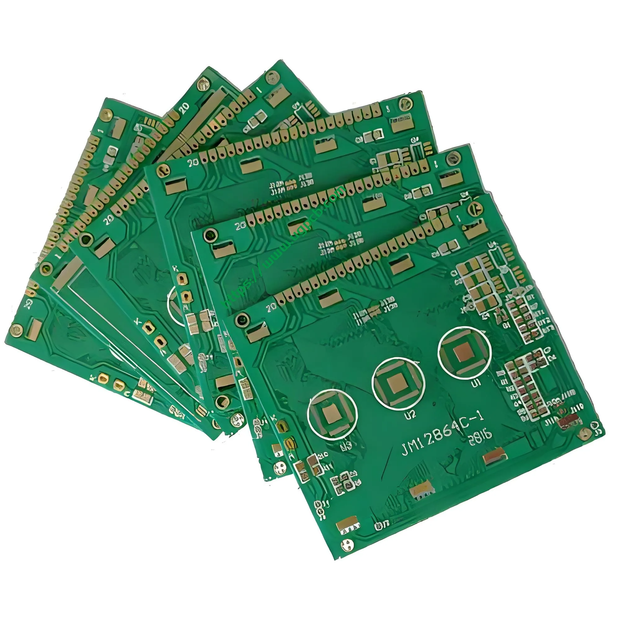
Descripción general del producto: Una solución de PCB de alta confiabilidad para el control de pantallas LCD
La UGPCB presenta laPlaca de circuito PCB con pantalla de cristal líquido LCD (Modelo: UGPCB-LCD-001), un alto rendimiento2-placa de circuito impreso rígida de capa FR-4 Diseñado específicamente para aplicaciones de control de pantallas de cristal líquido.. Este producto utiliza laminado revestido de cobre de alta gama Kingboard KB6165F como material base., con un espesor de tablero de 1.6 mm y 1 oz de lámina de cobre (aproximadamente 35 μm). El acabado superficial emplea elACEPTAR (Níquel químico/oro de inmersión) procesar en 2U” . El tablero mide 147.2 × 65 milímetros, con un diámetro mínimo de orificio de 0.22 mm y ancho/espaciado mínimo de línea de 0.3 milímetro/0,27 milímetro.
EstePCB con pantalla LCD Sirve como portador de circuito crítico que conecta los chips del controlador de pantalla a los paneles de cristal líquido.. Encuentra amplias aplicaciones en módulos de pantalla LCD de tamaño pequeño y mediano., pantallas de paneles de control industriales, pantallas del sistema de infoentretenimiento automotriz, e interfaces de interacción hombre-máquina para hogares inteligentes.
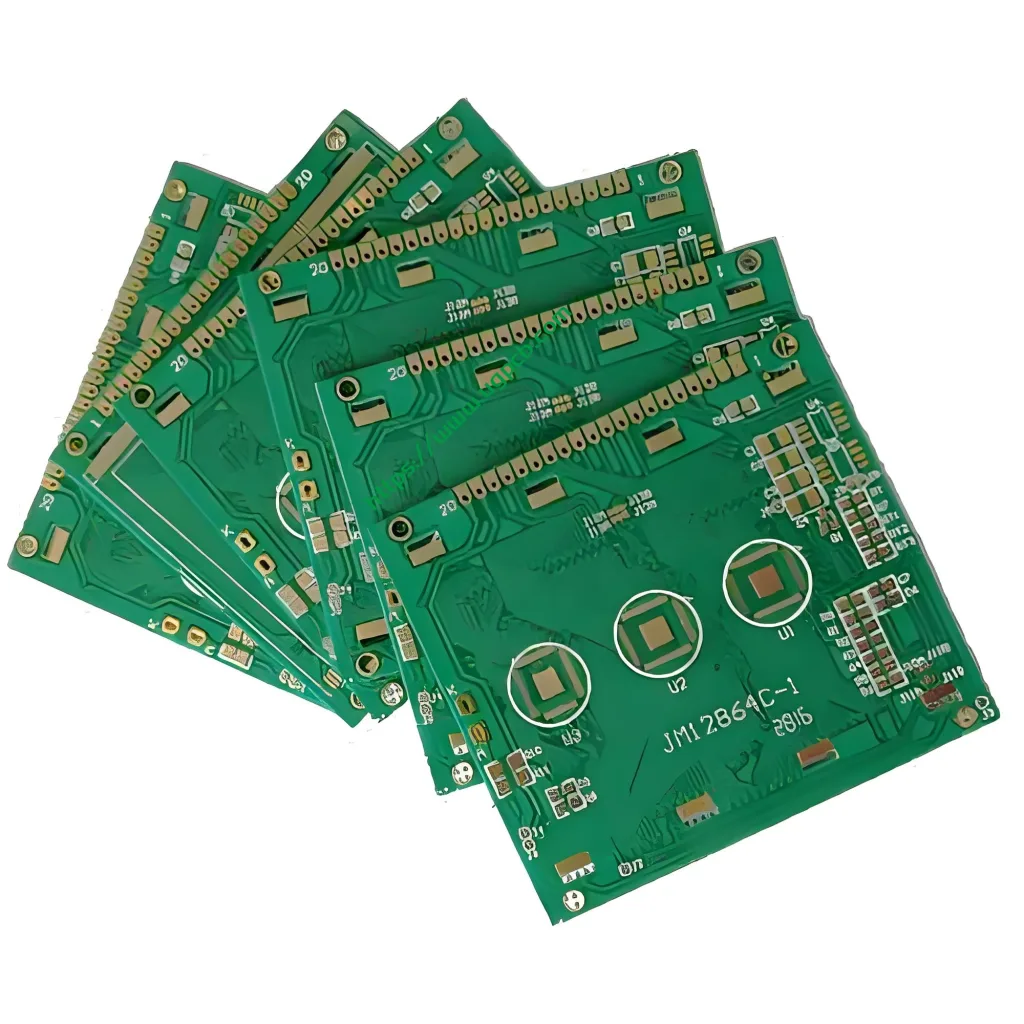
Definición del producto: ¿Qué es una PCB con pantalla de cristal líquido LCD??
Un PCB con pantalla de cristal líquido LCD (Placa de circuito impreso) Es una placa de circuito especializada diseñada para sistemas de conducción con pantalla de cristal líquido.. Realiza tres funciones principales.: transmisión de señal de conducción, distribución de energía, y enrutamiento de señales de control de sincronización. A diferencia del estándar placas de circuito impreso, un PCB con pantalla LCD exige tolerancias más estrictas en la precisión del ancho de línea, control de impedancia, y planitud de la superficie.
Este producto pertenece alPCB rígido de doble cara categoría con 2 capas (2l). Utiliza material retardante de llama de grado FR-4. (UL 94 V-0 calificado) y soporta tanto SMT (Tecnología de montaje en superficie) y procesos de ensamblaje híbrido de componentes de orificio pasante. La placa cumple con la clase IPC-6012. 2 requisitos de desempeño, haciéndolo adecuado para aplicaciones de electrónica industrial y electrónica de consumo..
Especificaciones de diseño: Parámetros críticos para la ingeniería de PCB LCD
Material de sustrato: La ventaja del KB6165F
Este producto utiliza laminado revestido de cobre Kingboard KB6165F, que ofrece las siguientes características clave de rendimiento:
- Temperatura de transición vítrea (tg): ≥150°C, Garantizar la estabilidad dimensional durante los procesos de soldadura por reflujo sin plomo.
- Temperatura de descomposición térmica (td): 325°C, proporcionando una excelente confiabilidad térmica
- Calificación de inflamabilidad: UL 94 V-0, con llama autoextinguible en el interior 10 segundos en pruebas de combustión vertical
- CTE (Coeficiente de expansión térmica): 12–15 ppm/°C en dirección X-Y, 40–230 ppm/°C en dirección Z, Ofrece una buena coincidencia térmica con los circuitos integrados del controlador LCD.
- c y f (Filamento anódico conductor) Resistencia: Excelente rendimiento anti-CAF que garantiza confiabilidad a largo plazo
- Compatible sin plomo: Cumple con los requisitos medioambientales RoHS
Según estándares de diseño IPC-2221, Los materiales con Tg ≥150°C son adecuados para procesos de montaje sin plomo., capaz de mantener la integridad estructural bajo temperaturas máximas de soldadura por reflujo que alcanzan 245–260 °C.
Diseño de recuento de capas y apilamiento
Las características del producto 2 capas (2l) con un estándar 1.6 mm de espesor del tablero. Para IPC-2221, 1.6 mm representa la especificación de espesor más comúnmente utilizada para rígidos. PCB, Equilibrando la resistencia mecánica con la comodidad del montaje..
Diseño de ancho y espaciado de línea
El ancho mínimo de línea de 0.3 mm y espacio mínimo entre líneas de 0.27 mm son parámetros cuidadosamente seleccionados paraPlaca controladora LCD Integridad de señal. Bajo estándares IPC-2221, el requisito de espacio mínimo para voltaje convencional (≤30V) los rastros de señales digitales son 0.1 milímetros (4 mil). este producto 0.27 milímetros (aproximadamente 10.6 mil) el espaciado supera con creces el requisito mínimo de IPC, proporcionando un amplio margen para la calidad de la señal.
Referencia de cálculo de diseño (basado en la fórmula simplificada de la capacidad de carga de corriente del conductor de la capa exterior IPC-2221):
Capacidad de transporte de corriente de traza de la capa exterior ≈ k × ΔT^0,448 × W^0,725 × T^0,725
donde k = 0.048 (para capa exterior). Con un aumento de temperatura de 10°C, a 0.3 mm traza con 1 oz de espesor de cobre ofrece una capacidad teórica de transporte de corriente de aproximadamente 1,2 a 1,5 A, suficiente para los requisitos de seguimiento de señal y alimentación de las placas controladoras LCD convencionales..
Diámetro mínimo del agujero
El diámetro mínimo del agujero de 0.22 milímetros (aproximadamente 8.7 mil) cae dentro de la categoría de perforación de precisión. Bajo IPC-6012, La tolerancia estándar del diámetro del orificio perforado es ±0,08 mm. (aproximadamente ±3 mil) . Para 0.22 mm microvías, Las tolerancias de fabricación normalmente se controlan dentro de ±0,05 mm..
Acabado superficial: ACEPTA que 2U”
ElACEPTAR (Níquel químico/oro de inmersión) acabado superficial con 2U” espesor de oro (aproximadamente 0.05 μm) cumple con los requisitos IPC-4552. IPC-4552 Revisión A (emitido en 2017) especifica el espesor del depósito de oro de 0.04 μm en 0.10 μm (1.6 μin en 4.0 mín.) y espesor de níquel de 3 μm en 6 μm.
Ventajas del acabado superficial ENIG:
- Excelente soldabilidad que admite múltiples ciclos de reflujo
- Fuerte capacidad de unión de cables
- Resistencia superior a la oxidación y la corrosión.
- Superficie plana adecuada para montaje de componentes de paso fino
- Vida útil extendida
Principio de funcionamiento: Mecanismos de transmisión de señal de la PCB de la pantalla LCD
ElPCB con pantalla de cristal líquido LCD opera en dos funciones principales: transmisión de señal ydistribución de energía.
1. Transmisión de señal del controlador de pantalla: Mostrar datos del chip controlador principal (MCU/SoC) viaja a través delplaca de circuito impreso a través de trazas de microstrip o stripline al IC del controlador LCD. El controlador IC convierte señales digitales en voltajes analógicos en escala de grises., que luego salen a través deltarjeta de circuito impresoLos finos rastros de los electrodos ITO en el panel de cristal líquido., controlar el ángulo de torsión de las moléculas de cristal líquido para producir la imagen mostrada.
2. Enrutamiento de la señal de control de sincronización: ElPCB con pantalla LCD lleva señales de sincronización críticas, incluido VSYNC (Sincronización vertical), HSYNC (Sincronización horizontal), DCLK (Reloj de píxeles), y DE (Habilitación de datos). El retraso de transmisión y la adaptación de impedancia de estas señales afectan directamente la calidad de la visualización..
3. Distribución de administración de energía: Elplaca de circuito LCD convierte la potencia de entrada (típicamente 3.3 V o 5 V) a través de circuitos de conversión DC-DC para generar los múltiples niveles de voltaje requeridos por el panel LCD, incluyendo VGH (voltaje de entrada, típicamente +15 V a +30 V), cf (tensión de cierre, normalmente −5 V a −15 V), y AVDD (tensión de alimentación analógica).
Clasificación de productos: Categorías de PCB LCD
PCB con pantalla de cristal líquido LCD se puede clasificar según las siguientes dimensiones:
Por recuento de capas
- Tableros de una sola cara: Se utiliza para pantallas LCD de código de segmento simple
- Tableros de doble cara (2l): La categoría de este producto, Se utiliza para controladores de pantalla TFT-LCD de tamaño pequeño y mediano.
- Tableros multicapa (4L y superior): Utilizado para alta resolución., módulos de visualización de gran formato
Por acabado superficial
- tableros ENIG: La categoría de este producto, ofreciendo el mejor rendimiento general
- tableros OSP: Menor costo, Adecuado para electrónica de consumo de ciclo de vida corto.
- tableros HASL: Adecuado para placas de controlador LCD con pasos de clavija más amplios
Por aplicación
- PCB LCD para electrónica de consumo: Pantallas secundarias de teléfonos inteligentes, pantallas de reloj inteligente, pantallas de lectores electrónicos
- PCB LCD de control industrial: IHM industriales, pantallas del panel de instrumentos, Controladores de pantalla del panel de operación CNC
- PCB LCD para automóviles: Sistemas de infoentretenimiento en el vehículo, grupos de instrumentos digitales, Tableros de control de pantalla HUD
- PCB LCD para dispositivos médicos: Monitores de pacientes, equipo de diagnóstico por ultrasonido, tableros de controlador de pantalla del sistema de imágenes médicas
Especificaciones de rendimiento principales
| Parámetro | Especificación | Estándar de referencia |
|---|---|---|
| Material laminado | KB6165F (tablero rey) | - |
| Tipo laminado | Laminado revestido de cobre de tela de vidrio FR-4 | UL 94 V-0 |
| Recuento de capas | 2 capas (2l) | - |
| Grosor del tablero | 1.6 milímetros | IPC-2221 |
| Espesor de cobre de la capa exterior | 1 onz (35 μm) | IPC-6012 Clase 2 |
| Acabado superficial | SOLO 2U” (0.05 µm Au) | IPC-4552 |
| Espesor de la capa de níquel | 3–6 µm (capa inferior) | IPC-4552 Rev A |
| Diámetro mínimo del agujero | 0.22 milímetros | IPC-6012 |
| Ancho mínimo de línea | 0.3 milímetros | IPC-2221 |
| Espacio mínimo entre líneas | 0.27 milímetros | IPC-2221 |
| Dimensiones del tablero | 147.2 × 65 milímetros | - |
| tg (Temperatura de transición vítrea) | ≥150°C | - |
| td (Temperatura de descomposición térmica) | 325°C | - |
| CTE (Dirección X-Y) | 12–15 ppm/°C | - |
| Calificación de inflamabilidad | UL 94 V-0 | UL 94 |
| Resistencia al arco | ≥60 segundos | - |
| Resistividad superficial | ≥2,6 × 10⁸ MΩ | - |
| Resistividad de volumen | ≥3,4 × 10⁹ MΩ·cm | - |
Análisis de la estructura del producto
ElPCB con pantalla de cristal líquido LCD La estructura comprende las siguientes capas desde el exterior hacia el interior.:
1. Capa exterior: acabado superficial ENIG: Capa de oro a 2U” (aproximadamente 0.05 μm) protege la capa subyacente de níquel de la oxidación. La capa inferior de níquel de 3 a 6 μm sirve como barrera de difusión entre el cobre y el oro..
2. Capa de lámina de cobre: 1 onz (aproximadamente 35 μm) lámina de cobre electrodepositada, grabado para formar el patrón del circuito.
3. Capa dieléctrica: Tela de vidrio grado FR-4 impregnada con resina epoxi., aproximadamente 0.7 mm de espesor (una sola capa), Proporcionar aislamiento eléctrico y soporte mecánico..
4. Capa de lámina de cobre: capa inferior 1 oz de cobre formando el patrón del circuito inferior.
5. Capa exterior: acabado superficial ENIG: Tratamiento ENIG simétrico a juego con la capa superior..
Características del producto: ¿Por qué elegir la PCB con pantalla LCD de UGPCB??
① Fabricación de alta precisión: Diámetro mínimo del agujero de 0.22 mm y ancho/espaciado mínimo de línea de 0.3 mm/0,27 mm admite los requisitos de enrutamiento de las placas de controlador LCD de alta densidad.
② Materiales de sustrato premium: Material FR-4 de alta gama Kingboard KB6165F con Tg ≥150°C y UL 94 V-0 La clasificación de inflamabilidad garantiza la compatibilidad del proceso sin plomo y la confiabilidad a largo plazo..
③ Acabado superficial estandarizado: SOLO 2U” El proceso cumple con IPC-4552., ofreciendo una excelente soldabilidad, resistencia a la oxidación, y vida útil prolongada.
④ Control de calidad riguroso: Los productos se someten a un control de calidad de proceso completo según la clase IPC-6012 2 estándares, tolerancia del diámetro del orificio de cobertura (±0,08 milímetros), espesor del cobre del agujero (≥20 µm), integridad de la máscara de soldadura, y pruebas eléctricas.
⑤ Diseño optimizado para LCD: control de impedancia, Integridad de señal, y la integridad de la energía están optimizadas específicamente para aplicaciones de control de pantallas de cristal líquido.
Proceso de fabricación: De la materia prima al producto terminado
UGPCB sigue un riguroso proceso de fabricación estándar paraPCB de pantalla LCD:
1. Corte de material →2. Transferencia de patrón de capa interior (Posicionamiento de brocas y marcas de registro.) →3. Perforación (diámetro mínimo del agujero 0.22 milímetros ± 0.08 milímetros) →4. Deposición/galvanoplastia de cobre no electrolítica (metalización de agujeros, espesor del cobre del agujero ≥20 μm) →5. Transferencia de patrón de capa exterior (ancho de línea 0.3 milímetros / espaciado 0.27 milímetros) →6. Patrón de revestimiento (acumulación de cobre 1 onz) →7. Aguafuerte →8. Impresión de máscara de soldadura →9. Acabado superficial ENIG (ACEPTAR, espesor oro 2U”) →10. Perfilado (dimensiones 147.2 × 65 milímetros) →11. Prueba eléctrica (100% prueba electrica) →12. Inspección final (AOI + inspección visual) →13. Embalaje y envío
Escenarios de aplicación típicos
📱 Electrónica de Consumo: Pantallas secundarias de teléfonos inteligentes, pantallas de reloj inteligente, PCB del controlador de pantalla del lector electrónico.
🏭Control Industrial: Interfaces hombre-máquina PLC (HMI), pantallas de instrumentos industriales, Tableros de controlador de pantalla de panel de operación CNC.
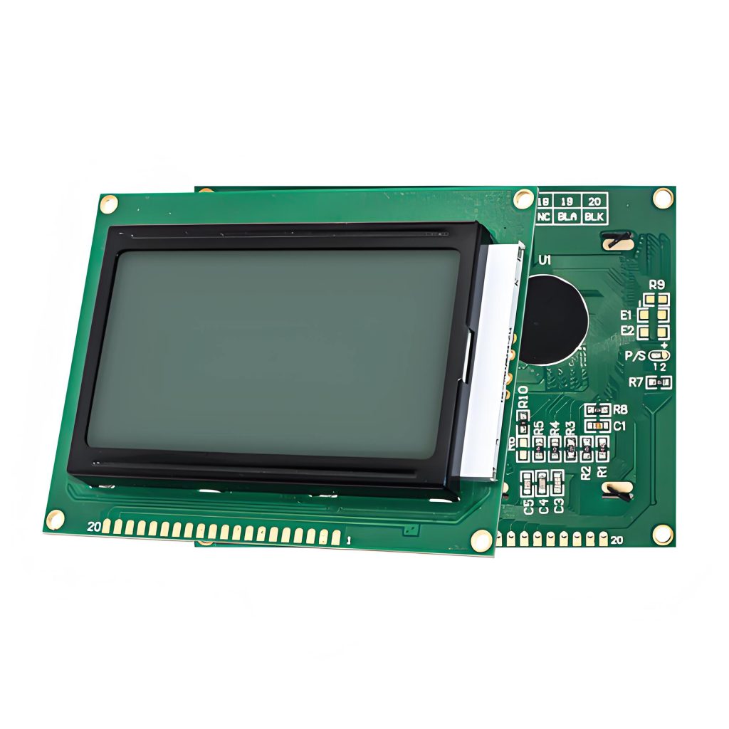
🚗 Electrónica automotriz: Sistemas de infoentretenimiento en el vehículo, grupos de instrumentos digitales, pantalla frontal (HUD) PCB de control de pantalla.
🏥 Dispositivos médicos: Monitores de pacientes, equipo de diagnóstico por ultrasonido, Placas de circuito del controlador de pantalla del sistema de imágenes médicas.
🏠 Hogar inteligente: Pantallas del sistema de control de acceso inteligente, paneles de control de electrodomésticos inteligentes, PCB del módulo de visualización del sistema de intercomunicación para edificios.
Por qué elegir UGPCB?
UGPCB trae años de PCB con pantalla LCD Experiencia en fabricación para cada proyecto.. Utilizamos materias primas de primera calidad como Kingboard KB6165F, hacer cumplir estrictamente la clase IPC-6012 2 estándares de calidad, y operar equipos de perforación y diseño de circuitos de alta precisión. Si necesitas Lcd Prototipos de PCB o producción en volumen, UGPCB ofrece alta precisión, soluciones de productos de alta confiabilidad.
📞 Obtenga su solución PCB para pantalla LCD hoy
UGPCB PCB con pantalla de cristal líquido LCD Se han implementado con éxito en numerosos sectores industriales., automotor, y proyectos de exhibición de electrónica de consumo.. Si necesitas Prototipos de PCB LCD para la validación del diseño o tarjeta de circuito impreso servicios de montaje llave en mano, UGPCB brinda soporte en todo el proceso, desde la fabricación de PCB hasta tarjeta de circuito impreso Ensamblaje SMT.
Póngase en contacto con el equipo profesional de UGPCB hoy para obtener su solución personalizada de PCB con pantalla LCD!
📧 Correo electrónico: [info@ugpcb.com]
📞 Teléfono: [+86-755-XXXXXXXX]
🌐 Sitio web: [www.ugpcb.com]
Atribución de fuente de datos
Las normas técnicas y los datos citados en este documento se derivan de las siguientes fuentes autorizadas.:
- IPC-6012 -Especificación de calificación y rendimiento para tableros impresos rígidos – Define las tolerancias del diámetro del orificio de la PCB (estándar ±0,08 mm), espesor del cobre del agujero (Clase 2 ≥20 µm), y requisitos de clase de rendimiento
- IPC-2221 -Norma genérica sobre diseño de tableros impresos – Especifica los requisitos de diseño de ancho/espaciado de línea y fórmulas de cálculo de capacidad de carga de corriente.
- IPC-4552 Revisión A (emitido 2017) -Especificación de rendimiento para níquel químico/oro por inmersión (ACEPTAR) Revestimiento para tableros impresos – Especifica los requisitos de espesor de depósito ENIG: níquel 3–6 μm, oro 0,04–0,10 μm
- UL 94 -Norma de seguridad de inflamabilidad de materiales plásticos para piezas de dispositivos y electrodomésticos –V-0 La clasificación requiere llama autoextinguible dentro 10 artículos de segunda clase
- Hoja de datos del producto Kingboard KB6165F – Parámetros técnicos del sustrato (Tg≥150°C, Td 325°C, UL 94 V-0, etc.)
- GB/T 4677 -Métodos de prueba para tableros impresos – Se utiliza junto con los estándares IPC como referencias de inspección.













