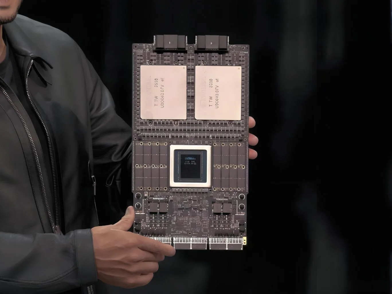
The orthogonal backplane PCB is a foundational component for next-generation AI computing clusters. Featuring a 78-layer structure within a two-centimeter profile and nearly one square meter of area, it enables direct interconnection of up to 576 GPU. 이것 고밀도 상호 연결 PCB solution for the NVIDIA Rubin Ultra architecture pushes the boundaries of conventional electronics manufacturing, demanding unprecedented precision in materials, 프로세스, 통합.

01 Architectural Shift: Why Orthogonal Backplanes Replace Traditional Cables
The move toward orthogonal backplane technology is a direct response to the limitations of copper cabling in massive AI systems. In a high-density setup like the NVL576 cabinet, a cable-based approach would necessitate over 20,000 individual cables, adding significant weight, complexity, and points of failure, while also suffering from signal degradation over distance.
대조적으로, 그만큼 “cable-less” orthogonal backplane integrates the interconnection network directly onto a massive, 다층 PCB. Computing and switch nodes connect orthogonally through this unified board via vertically stacked trays. 이것 advanced PCB technology streamlines the assembly process, potentially boosting efficiency by ~ 위에 40%, and solves the critical spatial challenge of linking thousands of components within a single rack.
02 Material Science Frontier: The M9 and PTFE Performance Dilemma
At the heart of this multilayer PCB 제조 challenge is the material itself. The Rubin architecture specifies an M9-grade high-speed laminate, chosen for its exceptional electrical properties: an ultra-low dielectric constant (DK) ~의 3.0 또는 더 적습니다 and a minimal dissipation factor (Df) ~의 0.0007 or below. Its coefficient of thermal expansion (CTE) is tightly controlled at ≤7 ppm/°C, which is crucial for dimensional stability.
A key innovation in M9 laminates is the use of quartz fiber (Q-cloth) instead of standard glass fiber. While this offers superior electrical performance, it creates immense PCB 제조 difficulties. Quartz fabric’s hardness drastically reduces drill bit life during the drilling process. Manufacturers must therefore adopt expensive diamond-coated drill bits or laser ablation systems, significantly elevating production costs.
To further optimize electrical performance in critical signal paths, a hybrid approach is often used. Sections of the board may incorporate PTFE (테프론), prized for its ultra-low loss, despite its much higher CTE. Managing the significant thermal expansion mismatch between these different materials—a CTE difference of nearly 30엑스—is a major hurdle in PCB lamination, requiring specialized bonding films and precise process controls to prevent delamination or warping under thermal stress.

03 Pushing Manufacturing Limits: 교련, 도금, and Layer Alignment
The physical scale and layer count of the orthogonal backplane create extreme PCB process challenges. A board thickness of 1-2 cm paired with via diameters often >0.2mm results in an extreme aspect ratio (board thickness to hole diameter) ~의 100:1 또는 그 이상.
This ratio poses severe problems for through-hole copper plating. As the aspect ratio increases, it becomes exponentially harder for plating solution to flow and deposit copper evenly deep within the holes. Advanced 맥박 도금 techniques are essential to achieve acceptable uniformity, preventing voids or weak connections that would compromise reliability.
뿐만 아니라, to maintain PCB signal integrity at high frequencies, any unused portion of a via (called a “stub”) must be removed through a precise back-drilling 프로세스. Achieving a back-drill depth tolerance within ±50 μm on a board of this size and complexity is an extraordinary feat of precision machining, involving highly sophisticated CNC systems and measurement technologies.
04 Engineering for Performance: Signal Integrity and Thermal Management
Ensuring clean signal transmission across 78 layers is paramount. This requires extremely tight 임피던스 제어, with tolerances within ± 5%, half the typical allowance for 표준 PCB. Every design element—trace width, 간격, dielectric thickness—must be meticulously calculated and executed.
At multi-gigabit data rates, physical effects like the 피부 효과, where current flows only on the conductor’s surface, increase resistance and must be accounted for in the design. 비슷하게, preventing 누화 between densely packed traces demands careful 스택업 디자인 and the use of ground planes for isolation.
PCB thermal management is an equally critical co-design challenge. While copper planes help spread heat, the insulating nature of the laminate core (with a thermal conductivity around 25 w/(m·K)) acts as a barrier. Effective heat dissipation from high-power components like GPUs often requires integrating metal thermal frames or cold plates directly into the PCB 조립, adding another layer of mechanical and thermal design complexity.
05 Supply Chain and Market Implications
The advent of orthogonal backplanes represents a significant value shift in the PCB 산업. The material cost and technical sophistication of these boards place them in a premium tier, creating high barriers to entry. Specialized materials like quartz fabric have limited global supply, concentrating manufacturing capability among a few leading PCB 공급 업체.
For companies that can master this advanced PCB technology, the opportunity is substantial. As AI server architectures evolve to adopt this form factor, demand for these sophisticated boards is projected to grow, creating a new high-margin segment within the high-frequency PCB 재료 and manufacturing market. This drives innovation across the supply chain, from laminate producers to equipment manufacturers.
06 The Future Trajectory of PCB Technology
The orthogonal backplane is a landmark in PCB development, but it is not the endpoint. The industry continues to research next-generation materials, such as modified hydrocarbons and other low-loss resins, to push signal loss and data rates even further.
The convergence of packaging and PCB technology is also accelerating. Concepts like embedded 구성 요소 그리고 substrate-like PCBs (SLP) blur the lines between traditional board manufacturing and semiconductor packaging, aiming to create ever-more integrated and efficient systems. Success in the orthogonal backplane domain provides the foundational expertise needed for these future advancements.
Mastering the orthogonal backplane is more than a manufacturing achievement; it is a declaration of technological capability in the AI era. It requires seamless integration of material science, precision engineering, and system-level design thinking. 을 위한 PCB 제조업체 and their clients, navigating these extreme challenges is the definitive pathway to powering the next leap in computational performance.
UGPCB 로고