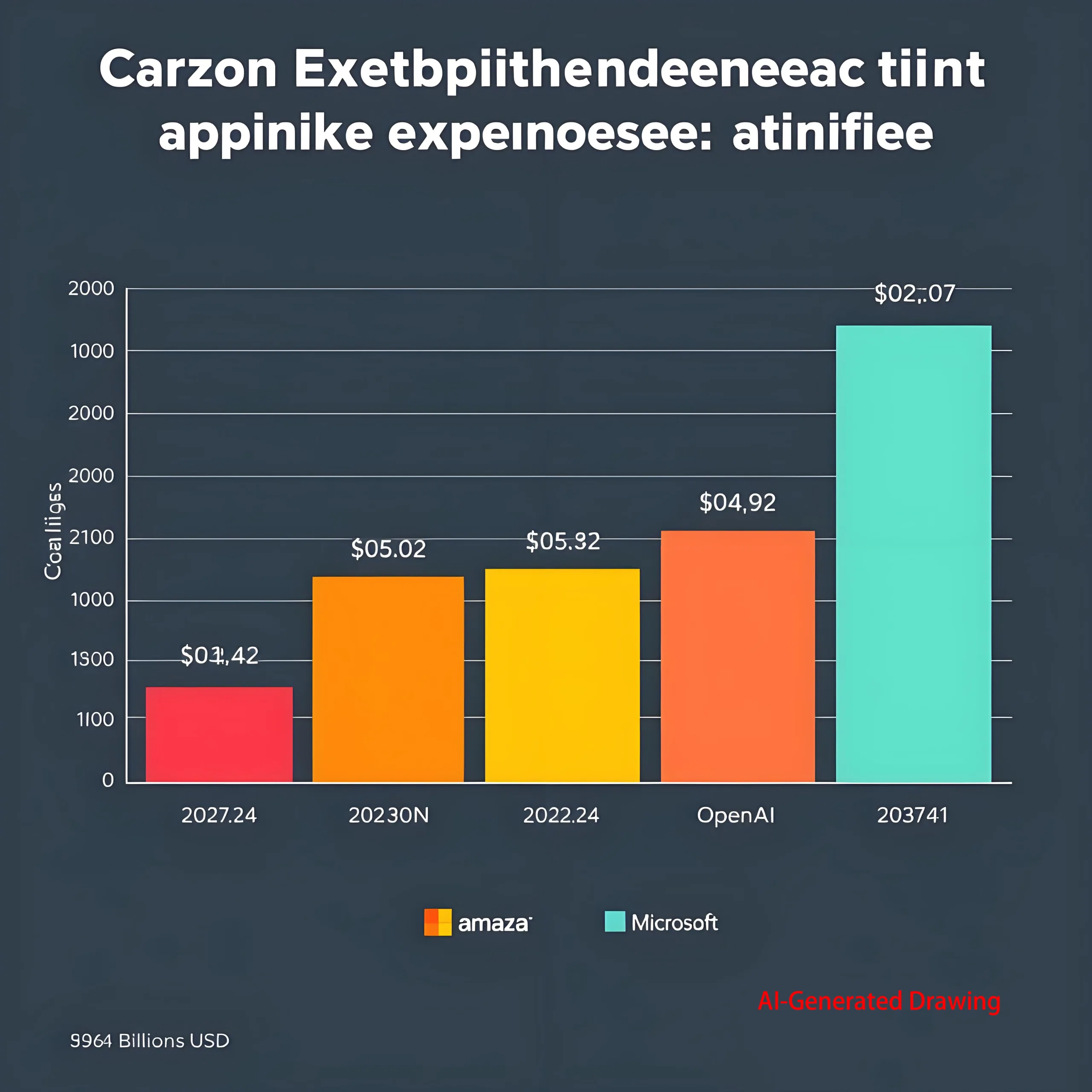
아마존이있을 때 $100 10억 2025 Capex는 OpenAi와 충돌합니다 “스타 게이트,” AI 구동 하드웨어 혁명은 광학 모듈과 PCB 핵심 엔진 역할을합니다.
글로벌 컴퓨팅 무기 경주: 자본 지출 환경
해외 거인: $100B+ Capex 서지
-
아마존: $75b capex 2024, 예상 >$100B 인사 2025 (구름 구동)
-
Google: $17.2b Q1 2025 capex (+44% 요), $75B 전년도 계획
-
마이크로 소프트: $16.7b Q1 2025 (+53% 요), AI 클라우드 투자 가속화
-
메타: capex $ 60-65B로 모금되었습니다 (llm r&디 + 맞춤형 하드웨어)
키 통계: 맨 위 4 CSP의 2025 총 Capex $ 300B를 초과합니다, 성장 >35% 요.
신흥 플레이어: 공격적인 새로운 참가자
-
Openai: “스타 게이트” 슈퍼 컴퓨터 프로젝트 (>$100b 추정 비용)
-
테슬라/애플: 사내 하드웨어 투자 급증 AI 칩
-
산업 변화: 맨 위 4 CSPS의 Capex 공유가 떨어집니다 59% (2023) 에게 <50% (2025)
“OpenAi가 구축함에 따라 SuperComputers와 Tesla는 Dojo 칩을 개발합니다, 전통적인 데이터 센터 경계가 무너지고 있습니다.”
AI 칩 전쟁: GPU 대. ASIC 전투
GPU: 컴퓨팅 제국의 기초
-
권세: 처리 >90% AI 모델 교육
-
성능 메트릭:
Compute Density (TFLOPS/mm²) = Transistor Count × Frequency × Core Efficiency -
Nvidia의 리드: H100 대역폭 3TB/s, NVLINK 속도 900GB/s
ASIC: 맞춤형 칩 혁명
-
전력 효율성: 40-60% 낮추다 전력 대. 동일한 계산에서 GPU
-
ROI 공식:
ROI (months) = (Power Savings × Scale) / (R&D Cost ÷ Lifespan) -
성장 투영: Marvell 예측 2028 당신은 ASIC 시장이 있습니다 >$40비 (47% cagr)
건축 혁명: 하이퍼 노드 클러스터
-
HWJ 384- 노드 클러스터:
Theoretical Compute = Single-Chip Power × 384 × Interconnect Efficiency (≈1.7×NVL72) -
GB200 제한: 구리 상호 연결 Max 72 카드, 광학은 토폴로지 장벽을 깨뜨립니다
PCB/광학 모듈: Compute Boom의 핵심 수혜자
AI 서버 PCB: 레이어 혁명 & 재료 혁신
| 서버 유형 | PCB 층 | 데이터 속도 | 가격 프리미엄 |
|---|---|---|---|
| 전통적인 | 6-8 | ≤56Gbps | 기준선 |
| GPU 서버 | 12-16 | 112Gbps | +300% |
| ASIC 노드 | 20+ | 224Gbps | +700% |
돌파구:
-
무거운 구리: 3오즈 포일 핸들 >1000에이 현재의
-
하이브리드 재료: 메가 트론 ™ 8 Df ≤0.0015 (@112GHz)
광학 모듈: CPO 대. LPO 기술 분할
-
수요 급증: >5,000 모듈 ASIC 클러스터 당
-
기술 경로:
-
LPO (선형 드라이브): 힘 ↓ 50%, 숨어 있음 <2ns
-
CPO (공동 포장 된 광학): 밀도 ↑ 5 ×, 비용 ↓ 30%
-
-
시장 크기:
Optical Market = AI Chip Volume × Interconnect Ratio × Penetration Rate
주요 예측: 1.6t에 도달 할 모듈 채택 25% ~에 의해 2025 (경력)
중국의 상승: 현지화 혁신
정책 중심 컴퓨팅 인프라
-
국가 허브: 70+ 건설중인 데이터 센터, 600K+ 새로운 랙
-
대상 계산: 1,037.3 eflops by 2025 (43% 성장)
하드웨어 현지화: PCB/광학 진행
| 분절 | 현지화율 | 지도자 | 혁신 |
|---|---|---|---|
| 고속 PCB | 35% | UGPCB / Deepkin / Tech | 112GBPS 초 저 손실 |
| 광학 모듈 | 60%+ | innolight/eoptolink | 1.6T CPO 대량 생산 |
| IC 기판 | <15% | UGPCB/sinxing | 2.5D TSV 포장 |
관세 영향: 고급 PCB 재배치 비용 >30%, 지역 공급망 강화
투자 초점: 리더 분석
PCB 제조업체의 위치
-
UCP : Core Nvidia HGX 기판 공급 업체, 생산하다 >95%
-
그리고 기술: M7 등급 재료 Nvidia 인증, 급격한 공유
-
딥킨: 3디 기판 용량 ↑ 300%
광학 모듈 공급 업체 환경
| 공급업체 | 핵심 기술 | 800G 상태 | 1.6t 진보 |
|---|---|---|---|
| 인노 라이트 | LPO + 실리콘 광자 | 양산 | 견본 추출 |
| eoptolink | CPO 통합 | 작은 배치 | 실험실 단계 |
| 케임브리지 기술 | 얇은 필름 린보 | 테스트 | - |
장비 & 재료 챔피언
-
Nikon Precision: 직접 영상 리소그래피 ≤2μm
-
송곳니 뱅: 초박형 차폐 필름 ≤5μm
-
Wazam 새로운 재료: 낮은 DK/DF와 같습니다 메가 트론 8
2025-2028 기술 로드맵
-
PCB 레이어 스케일링:
Avg AI Server Layers = 12 + 0.5×(Annual Compute Growth)→ 24L BY 2028 -
광학적 통합:
-
CPO 채택 >15% ~에 의해 2025
-
온보드 광학 (오보) 생산 2027
-
-
열 혁신:
-
액체 냉각 PCB 열 저항 <0.1° C/W
-
위상 변경 재료 전도도 >20w/mk
-
업계 통찰력: “컴퓨팅 수요가 분기별로 두 배가됩니다, PCB의 빛 경로를 에칭하고 3D 실리콘 도시를 구축하는 것만으로 만 Ai Tsunami를 탈 수 있습니다.”