
UGPCB 18층 서버 PCB: 고성능 컴퓨팅을 위해 설계됨 & 데이터 센터
데이터센터와 클라우드 컴퓨팅 시대, 서버 안정성과 성능은 디지털 비즈니스 운영에 매우 중요합니다.. 기본적인 하드웨어 캐리어로서, 정밀한 디자인과 뛰어난 품질의 서버 PCB (인쇄 회로 기판) 가장 중요하다. 심층적인 산업 전문 지식과 최첨단 기술 활용, UGPCB 고성능을 제공합니다, 차세대 데이터 센터 애플리케이션의 가장 까다로운 요구 사항을 충족하는 매우 안정적인 18레이어 서버 PCB.

제품개요 & 정의
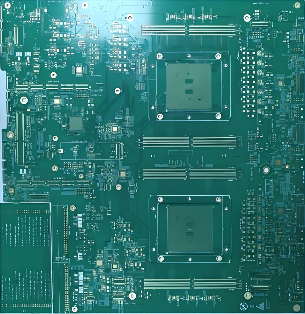
서버 PCB는 서버 마더보드의 핵심 구성 요소입니다., 스토리지 백플레인, 그리고 다양한 기능성 도터카드. CPU와 같은 중요한 구성 요소를 호스팅합니다., 메모리, 및 칩셋, 고속 신호 전송 촉진, 전력 분배, 및 시스템 상호 연결. 고성능 애플리케이션 서버용으로 특별히 설계됨, 본 UGPCB 제품은 18단 고다층 구조를 활용하고 기판 두께를 2.4mm±10%로 강화한 제품입니다., 대규모 데이터 세트를 처리하고 고속 계산을 지원하기 위한 강력한 하드웨어 기반 역할을 합니다..
핵심 디자인 하이라이트 & 기술 분석
서버 플랫폼을 다루기 위해’ 신호 무결성에 대한 극단적인 요구, 전력 무결성, 열 관리, 이 제품은 여러 핵심 기술을 통합합니다.:
-
고급 스택업 & 재료:
-
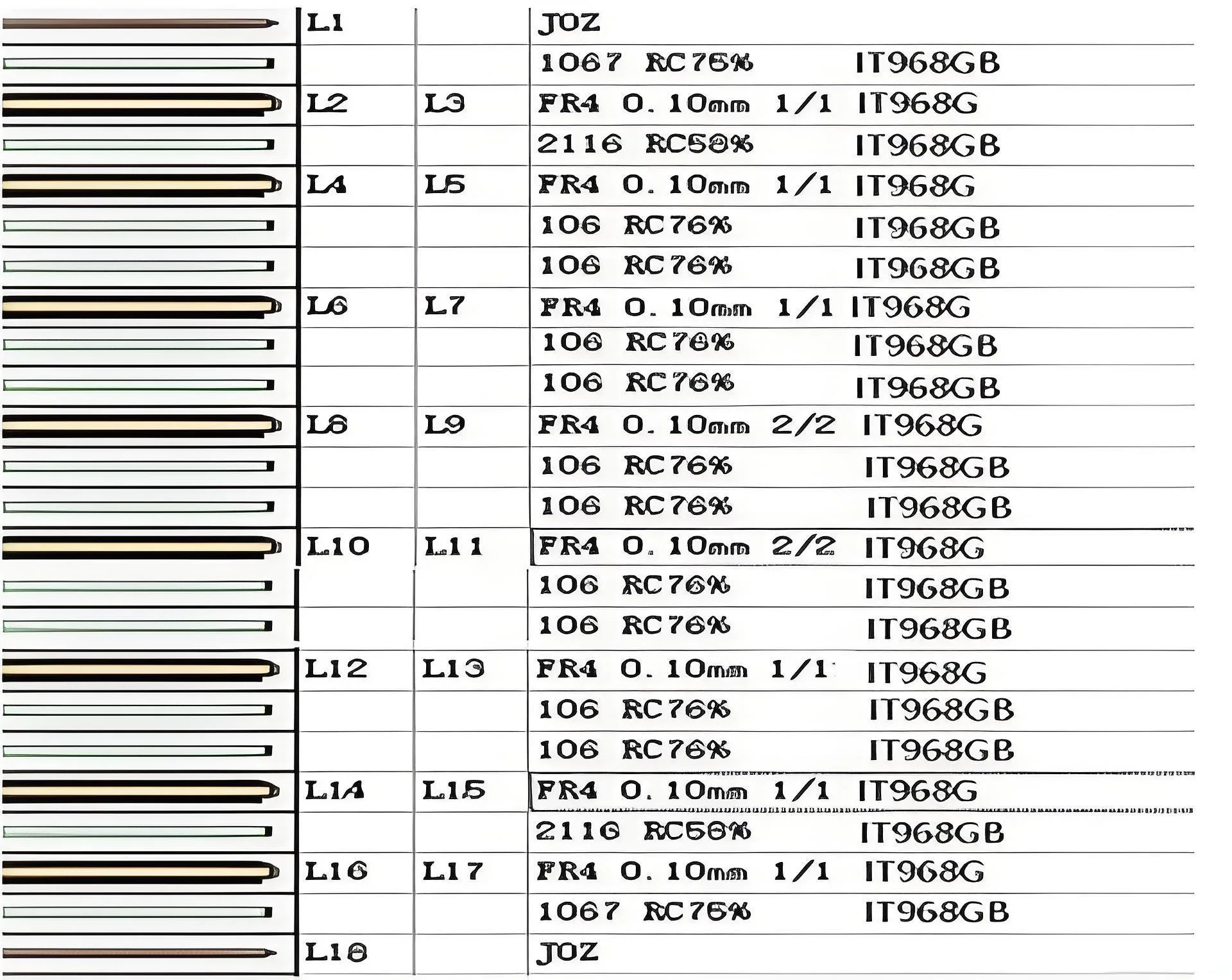
라미네이트: ITEQ IT968G 고속 활용, 저손실 재료. Tg가 높다 (유리전이온도) 장기간 고온 서버 작동 시 치수 안정성과 일관된 전기적 성능을 보장합니다., 효과적으로 신호 전송 손실을 감소.
-
레이어 & 구리 무게: 세심하게 설계된 하이브리드 구리 중량 방식을 갖춘 18층 복합 스택업 (일부 내부 레이어에 2Oz 두께의 구리 호일이 특징). 이는 전력 평면의 전류 전달 용량과 열 성능을 최적화하는 동시에 고속 신호 레이어에서 미세한 라우팅을 가능하게 합니다..
-
-
정밀 라우팅 & 상호 연결:
-
라인 성능: 0.1mm/0.1mm의 초미세 선폭/간격 실현, 고밀도 BGA 패키지에 대한 팬아웃 및 상호 연결 요구 사항 충족 (예를 들어, CPU, GPU, FPGA).
-
마이크로 비아 기술: 0.20mm의 최소 기계식 드릴 직경을 지원합니다., 라우팅 밀도 및 공간 활용도 향상.
-
-
신호 무결성을 위한 핵심 기술:
-
백 링: 고속 차동 신호용 (예를 들어, PCIE, SAS, 이더넷), 백 드릴링 공정을 통해 스루홀에서 사용되지 않은 구리 스텁을 제거합니다., 신호 반사 및 감쇠를 크게 줄입니다.. 이는 신호 품질을 보장하기 위한 핵심 프로세스입니다. 고속 PCB.
-
RTF 구리 포일: 역처리 포일 사용, 보다 매끄러운 구리 표면을 제공합니다.. 이는 고주파 신호에 대한 표피 효과 손실을 효과적으로 줄입니다., 신호 전송 효율 향상.
-
-
안정적인 표면 마감:
-
무전해 니켈 침지 금 (동의하다) 최종 표면처리로 적용됩니다.. ENIG는 평평한 표면을 제공합니다, 우수한 납땜성, 안정적인 접촉 인터페이스, 및 장기 산화 저항성, 밀도가 높은 납땜에 이상적입니다., 미세 피치 구성 요소 서버 PCB에.
-
제품 기능 & 장점
-
탁월한 전기적 성능: 백 드릴링 및 RTF 포일과 결합된 고속 IT968G 라미네이트로 저손실 보장, 고주파 신호의 저지연 전송, 이상적인 선택이 되도록 고주파 PCB 그리고 고속 PCB.
-
뛰어난 파워 핸들링 & 열 관리: 2Oz 내부층 구리 및 2.4mm 보드 디자인으로 전류 전달 용량 향상, 전반적인 구조적 강성, 및 열전도도.
-
고밀도 & 신뢰할 수 있음: 0.1/0.1mm 선폭/공간과 결합된 18레이어 라우팅 공간은 가장 복잡한 설계를 지원합니다.. 엄격한 공정 제어와 높은 Tg 재료로 장기적인 신뢰성을 보장합니다. 24/7 중단없는 운영.
-
엔드투엔드 서비스 지원: UGPCB는 최고 수준뿐만 아니라 PCB 제조 설계 검토부터 생산까지 원스톱 솔루션, 시장 출시 기간 단축.
생산 공정 개요
우리의 제조는 엄격한 기준을 준수합니다 IPC 표준 품질 관리 시스템:
엔지니어링 검토 → 재료 준비 → 내부 레이어 이미징 → 적층 → 드릴링 & 백 드릴링 → 홀 금속화 → 외부 레이어 이미징 → 도금 (하이브리드 구리 중량용) → 솔더 마스크 적용 (프리원) → ENIG → 라우팅 / 프로파일링 → 전기 테스트 & 최종검사
https://via.placeholder.com/800×450.png?text=18층+PCB+단면
대체 텍스트: 18단 서버 PCB 기판의 단면도, 고속 신호 전송을 위한 정밀한 라미네이션 및 백드릴 비아 구조를 자세히 설명합니다..
응용 & 분류
이 고성능 PCB는 다음과 같이 널리 사용됩니다.:
-
기업 & 클라우드 서버 마더보드
-
데이터센터 AI 컴퓨팅 가속 카드
-
고성능 스토리지 서버 & 백플레인
-
네트워크 스위치 & 통신장비 코어보드
기술 분류:
-
레이어 수에 의해: 높은 다층 PCB (18 레이어)
-
기술 별: 고속/고주파 PCB, 백 드릴 PCB, 무거운 구리 PCB
-
응용 프로그램에 의해: 서버/데이터센터 PCB
-
표면 마감별: 동의하다 (무전해 니켈 침지 금) PCB
UGPCB를 선택하십시오, 고품질 서버 PCB 보드 그 이상을 선택하세요; 고급 PCB 제조 분야에서 신뢰할 수 있는 파트너를 얻습니다.. 우리는 복잡한 기술 세부 사항을 귀하의 제품에 대한 신뢰할 수 있는 이점으로 변환하는 데 최선을 다하고 있습니다., 차세대 데이터 센터 솔루션 강화.
맞춤형 PCB 솔루션 견적 및 기술 상담을 원하시면 지금 당사 전문가 팀에 문의하세요.!


