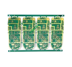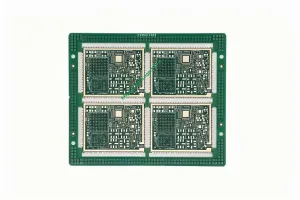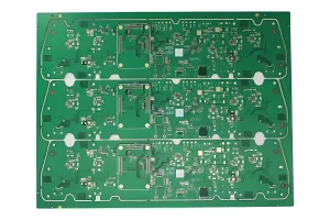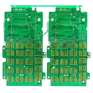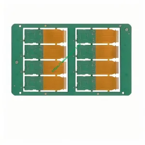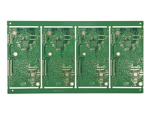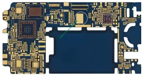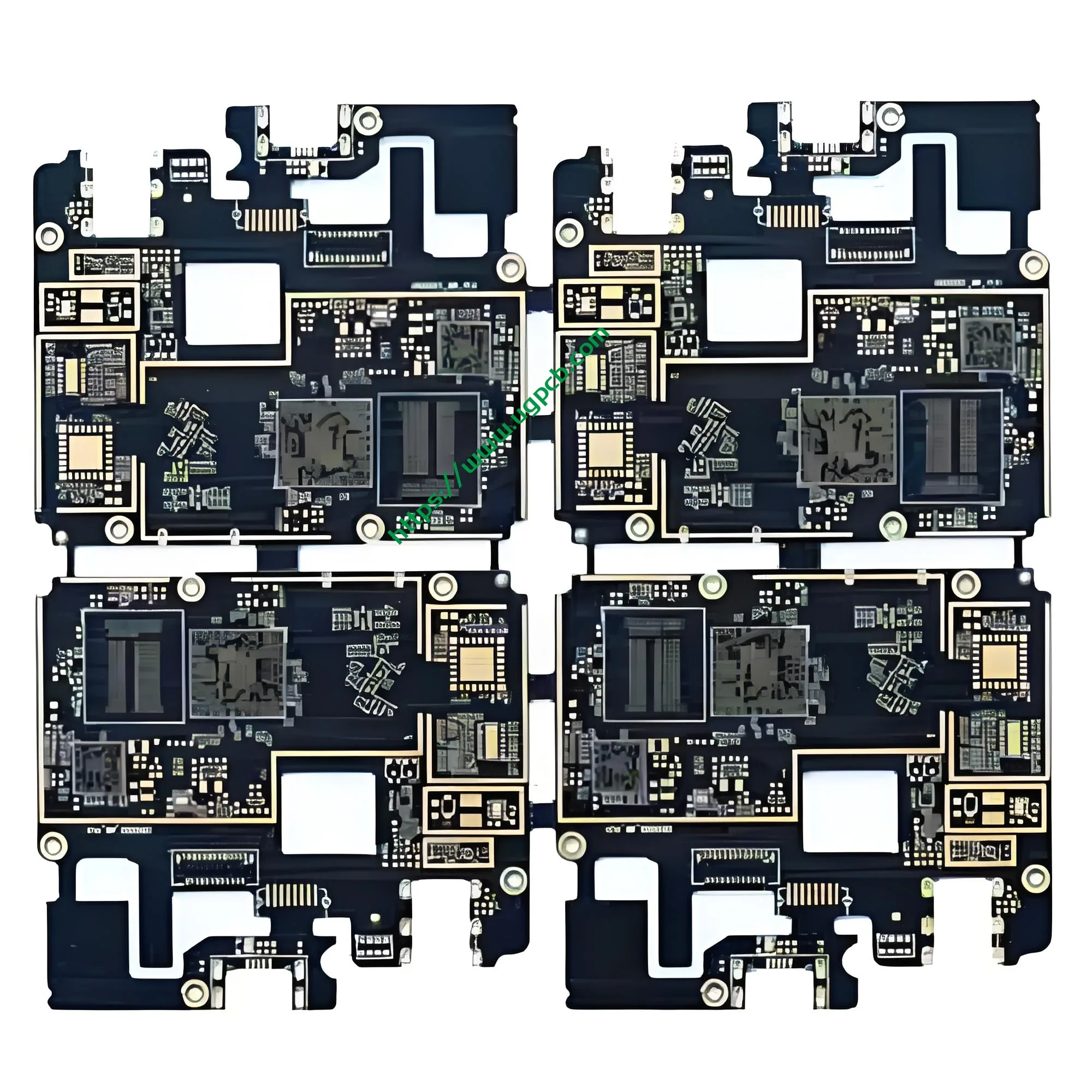
제품개요
UGPCB는 다음을 소개합니다. 6‑layer 2+N+2 HDI PCB (모델: 6패 2+N+2 HDI PCB). This high‑density interconnect 인쇄 회로 기판 is engineered specifically for communication equipment. It uses ITEQ IT150 high‑performance laminate, combined with a second‑order HDI build‑up architecture, 2.5mil/2.5mil fine‑line trace and space, 그리고 0.1mm 레이저 마이크로비아. These features deliver reliable interconnections for 5G base stations, high‑speed network switches, 광학 모듈, 그리고 유사한 응용 프로그램.
에서 PCB 산업, HDI (고밀도 상호 연결) technology is the core enabler for shrinking component pitches and rising signal speeds. 그만큼 2+N+2 HDI PCB architecture represents the second‑order HDI category. It achieves an optimal balance among routing density, 신호 무결성, 그리고 제조비용.
What Is a 2+N+2 HDI PCB?
Definition and Nomenclature
“2+N+2” is a standardized naming convention for HDI stack‑up structures. It is defined in theIPC‑2226 standard and is classified asIII 형 within that system.
Breaking down the term:
- 그만큼 first “2” means two sequential build‑up layers above the core.
- “N” stands for the number of core layers (here N=2, 즉., two inner core layers).
- 그만큼 second “2” means two sequential build‑up layers below the core.
따라서, a 2+N+2 structure adds two build‑up layers on each side of the conventional core. These are constructed throughtwo sequential lamination cycles. This 6‑layer board therefore comprises: 2 외부 빌드업 레이어 + 2 inner core layers + 2 외부 빌드업 레이어.

IPC‑2226에 따른 HDI 분류
The IPC‑2226 standard defines several HDI types based on microvia structures and build‑up layer counts:
| HDI 유형 | 구조 | Build‑up Layers (면당) | Minimum BGA Pitch | 일반적인 응용 프로그램 |
|---|---|---|---|---|
| I 형 I | 1+N+1 | 1 층 | 0.5mm | 스마트폰, mid‑density designs |
| 유형 II/III | 2+n+2 | 2 레이어 | 0.4mm | 네트워킹 장비, high‑performance computing |
| III 형 / 엘릭 | 3+N+3 and above | 3+ 레이어 | 0.3mm and below | 플래그십 스마트폰, AI modules |
This product falls into the2+N+2 category. It features two build‑up layers per side, with microvias that can be arranged in eitherstacked or staggered 구성.
핵심 기술 사양
| 매개 변수 | 사양 |
|---|---|
| 모델 | 6패 2+N+2 HDI PCB |
| 재료 | ITEQ IT150 |
| 레이어 수 | 6 레이어 (2+N+2 second‑order HDI) |
| 솔더 마스크 색상 | Black or White (선택 과목) |
| 완성된 보드 두께 | 1.0mm |
| 내층 구리 두께 | 1 온스 (~35μm) |
| 외층 구리 두께 | 0.5 온스 (~17.5μm) |
| 최소 추적 / 간격 | 2.5밀 / 2.5밀 (~63.5μm / ~63.5μm) |
| Minimum Mechanical Drill | 0.2mm |
| Minimum Laser Drill | 0.1mm |
| 표면 마감 | 이머젼 골드 + OSP |
| 기본 애플리케이션 | 통신 장비 |
Material Deep Dive: ITEQ IT150
Material Positioning
ITEQ IT150 는 medium‑Tg, 할로겐 프리, multifunctional epoxy 라미네이트. It sits between standard FR-4 and high‑performance low‑loss materials. It delivers lead‑free process compatibility, good manufacturability, and cost‑effectiveness.
The IT150GS variant (within the IT150 family) is a medium‑Tg (Tg >150DSC에 의한 ° C), 할로겐 프리, middle‑loss material. It offers high thermal reliability and excellent CAF resistance. It is specifically designed for server, 저장, and networking applications.
핵심 성능 매개 변수
Based on ITEQ official datasheets and IPC‑TM‑650 test methods:
| 재산 | 테스트 방법 | 전형적인 가치 | 단위 |
|---|---|---|---|
| 유리전이온도 (Tg) | DSC (IPC‑2.4.25) | 155 | ℃ |
| 분해 온도 (Td, 5% WT 손실) | TGA (IPC‑2.4.24.6) | 365 | ℃ |
| Z축 CTE (A1, Tg 이하) | IPC‑2.4.24 | 35–40 | ppm/°C |
| Z축 CTE (A2, Tg 이상) | IPC‑2.4.24 | 220–240 | ppm/°C |
| X/Y‑axis CTE (40–125°C) | IPC‑2.4.41 | 11/13 | ppm/°C |
| 유전 상수 (DK) @ 1GHz | IPC‑2.5.5.13 | 4.2–4.5 | - |
| 소산 인자 (Df) @ 1GHz | IPC‑2.5.5.13 | 0.010–0.018 | - |
| T288 Thermal Stress | IPC‑TM‑650 | >60 | Minutes |
| 수분 흡수 | IPC‑2.6.2.1 | 0.12 | % |
| 가연성 등급 | UL94 | V-0 | 평가 |
| UL MOT (Max Operating Temp) | - | 130 | ℃ |
물질적 이점
1. Lead‑Free Process Compatibility
Standard FR‑4 typically has a Tg around 130°C. ITEQ IT150이 제공하는155℃. Under lead‑free reflow peaks of260℃, this higher Tg provides superior dimensional stability. The material resists excessive Z‑axis expansion, which significantly reduces the risk of via barrel cracking and pad lifting during assembly.
2. 우수한 CAF 저항
CAF (전도성 양극 필라멘트) is a primary failure mode in PCBs. It occurs when electrochemical migration creates short circuits under humid and hot conditions. ITEQ IT150 offershigh CAF resistance (18엘 / less than 100mil). This makes it especially suitable for long‑term outdoor deployment in communication infrastructure.
3. Halogen‑Free Compliance
ITEQ IT150 meetsJPCA‑ES‑01‑2003 halogen‑free standards. Chlorine (Cl) 그리고 브롬 (Br) content are each below 0.09% 체중. Total Cl+Br is below 0.15% (1500ppm).
설계 지침
Stack‑Up Architecture
The 2+N+2 HDI PCB is manufactured throughsequential lamination:
- Core fabrication – Start with a double‑sided copper‑clad laminate. Etch inner layer circuits, perform mechanical drilling (0.2mm), and plate to create buried via connections.
- First build‑up – Apply prepreg and copper foil (or RCC) to both sides of the core. Execute the first lamination cycle.
- First laser drilling – Drill first‑order blind vias (laser holes at 0.1mm) and fill them with copper.
- Second build‑up – Apply additional dielectric layers and copper foil. Execute the second lamination cycle.
- Second laser drilling – Drill second‑order blind vias (0.1mm) and fill with copper.
- 외부 레이어 회로 – Form outer layer circuits (trace/space 2.5mil) and apply the surface finish.
이것two‑sequential‑lamination process is precisely what the “2” in 2+N+2 signifies.
Fine‑Line Circuit Design
이 제품은 2.5밀/2.5밀 (~63.5μm/63.5μm) 트레이스 폭과 간격. This exceeds the HDI 디자인 Level C (60‑99μm) defined in IPC‑2226. This fine‑line capability enables:
- 0.4mm 피치 BGA breakout with ample routing channels.
- Flexible signal routing for high‑density 요소 놓기.
- Reduced layer count, which lowers overall PCB cost.
마이크로 비아 기술
이 제품은hybrid drilling approach:
- 기계식 드릴링 – 최소 직경 0.2mm, used for through‑holes and buried vias in the core.
- 레이저 드릴링 – 최소 직경 0.1mm (4밀) , used for blind vias in build‑up layers.
The 0.1mm laser microvia reduces via area by75% compared to a 0.2mm mechanical hole. This significantly frees up routing space. It is fundamental to achieving high‑density interconnect and enabling비아인패드 designs for fine‑pitch BGAs.
작동 원리
The 2+N+2 HDI PCB works through amulti‑layer interconnect architecture:
- Core‑layer interconnection – Buried vias, 에 의해 형성 기계적 드릴링 + 도금, connect signals between core layers.
- Build‑up interconnection – Blind vias, 에 의해 형성 레이저 드릴링 + 도금, connect outer signal layers to inner layers.
- Full‑board through‑holes – After stack‑up completion, mechanical drilling penetrates all layers to create through‑holes.
- Signal transmission path – High‑speed signals travel from surface BGA pads → through laser blind vias into inner layers → across buried vias through the core → through laser blind vias on the opposite side to the bottom layer.
이것stepped interconnect structure shortens signal paths and reduces parasitic via effects. 결과적으로, it preserves high‑speed signal integrity.
성능상의 이점
열 신뢰성
ITEQ IT150’sTd (decomposition temperature) reaches 365°C, which is well above the lead‑free reflow peak of 260°C. T288 thermal stress testingexceeds 60 분 without delamination. This ensures material integrity through multiple reflow cycles.
신호 무결성
1GHz에서, ITEQ IT150 exhibits a dielectric constant Dk of approximately 4.2–4.5 and a dissipation factor Df of 0.010–0.018. As a “standard‑to‑mid‑loss” material, IT150 provides a compelling price‑performance ratio compared to ultra‑low‑loss materials. This makes it ideal for production‑ready communication equipment.
기계적 강도
ITEQ IT150이 제공하는flexural strength of 470–500 N/mm² in the warp direction and 400–430 N/mm² in the fill direction. This ensures structural integrity throughout assembly and field deployment.
제품 분류
This product is classified across multiple dimensions:
| Classification System | 범주 |
|---|---|
| IPC‑2226 HDI Type | 유형 II/III (2+n+2, double build‑up per side) |
| HDI Order | Second‑order (2 laser drilling cycles + 2 lamination cycles) |
| Rigid/Flexible | 강성 PCB |
| 레이어 수 | 6‑레이어 다층 보드 |
| 재료 시스템 | Medium‑Tg, 할로겐 프리, FR‑4‑compatible epoxy |
| 표면 마감 | 이머젼 골드 + OSP hybrid finish |
| 애플리케이션 도메인 | Communication‑grade PCB |
제조 공정 흐름
UGPCB follows this production sequence for the 6‑layer 2+N+2 HDI PCB:
단계 1: Core Layer Fabrication
Material cutting → Inner layer dry film → Etching → AOI inspection → Brown oxide treatment
단계 2: First Build‑Up
라미네이션 (핵심 + 준비 + 구리박) → First lamination → First‑order laser drilling (0.1mm) → 디스미어 → 무전해 구리 + 도금 → 회로 패터닝
단계 3: Second Build‑Up
Second lamination → Second lamination → Second‑order laser drilling (0.1mm) → 디스미어 → 무전해 구리 + 도금 → 회로 패터닝
단계 4: Outer Layer and Finishing
기계식 드릴링 (0.2mm through‑holes) → Electroless copper + plating → Outer layer circuits (2.5밀/2.5밀) → Solder mask → Immersion Gold + OSP surface finish → Electrical testing → Final inspection → Packaging and shipment
The entire process involvestwo lamination cycles and two laser drilling operations. This demands exceptional process control and precision.

응용 시나리오
This product is primarily designed for통신 장비:
5G 커뮤니케이션 인프라
- 5G 기지국 (gNB) – RF front‑end and baseband processing units.
- High‑speed backplane interconnects for 5G network equipment.
- Enterprise‑grade routers and core switches.
High‑Speed Data Transmission
- 400G/800G optical modules – control and signal processing boards.
- High‑speed fiber‑optic switches.
- 광학 트랜시버.
Other High‑End Applications
- High‑performance servers and storage devices.
- AI inference/training accelerator cards.
- Advanced medical imaging equipment.
The 2+N+2 HDI structure is particularly well‑suited formoderate pin‑count, high‑density BGA 라우팅. It enables complex signal interconnects within limited board space.
UGPCB를 선택하는 이유는 무엇입니까??
UGPCB brings deep manufacturing expertise to HDI PCB production:
- Fine‑line capability – 2.5mil/2.5mil trace/space in volume production, meeting advanced HDI design requirements.
- Mature microvia process – 0.1mm laser via + 0.2mm mechanical drill hybrid solution with stable yield.
- Comprehensive material certification – Full qualification on ITEQ IT150 and other mainstream material systems.
- End‑to‑end process control – Every step from cutting to electrical testing strictly follows IPC‑6012 rigid PCB qualification and performance specifications.
- Communication industry track record – Extensive experience in 5G base station, optical module, and network equipment PCB 제조.
지금 견적을 요청하세요
Whether you are designing high‑speed backplanes for 5G base stations or developing next‑generation optical modules, UGPCB’s 6‑layer 2+N+2 HDI PCB provides the reliable interconnect foundation your project deserves.
데이터 소스 선언
The technical data cited in this document comes from the following authoritative standards and sources:
- IPC‑2226 - Sectional Design Standard for High Density Interconnect (HDI) 인쇄보드
- IPC‑6012E/F - 경질 인쇄 기판의 자격 및 성능 사양
- IPC/JPCA‑2315 - Design Guide for High Density Interconnect Structures and Microvias
- ITEQ IT‑150 / IT‑150GS Official Datasheets and Material Specifications
- IPC‑TM‑650 – Test Methods Manual (including methods 2.4.4, 2.4.24, 2.4.24.6, 2.4.25, 2.5.5.13, 2.6.2.1, 그리고 다른 사람들)
- JPCA‑ES‑01‑2003 - Halogen‑Free Copper‑Clad Laminate Standard
- UL94 - 기기 및 가전제품 부품용 플라스틱 재료의 가연성 안전에 관한 표준