

Professional 6-Layer ENIG PCB Product Overview and Definition
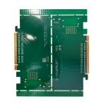
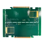
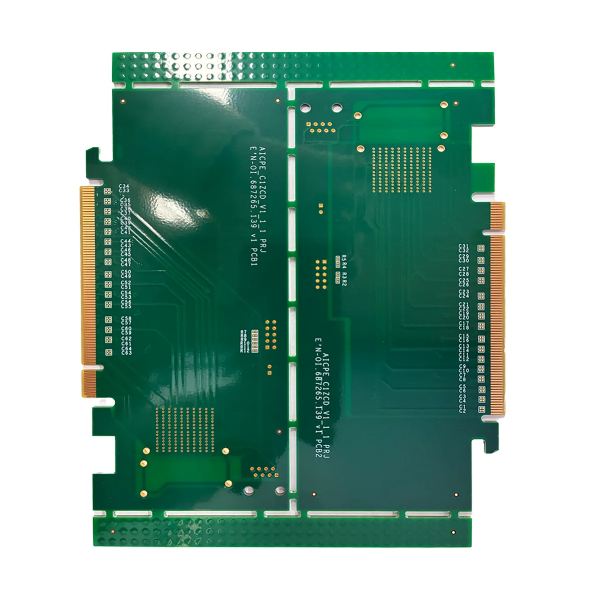
그만큼 6-레이어 견고한 PCB from UGPCB is a 다층 인쇄 회로 보드 manufactured using standard TUC TU768 TG180 core material based on FR-4. This circuit board features a standard thickness of 1.60mm 그리고 2μm Electroless Nickel Immersion Gold (동의하다) 표면 마감, with dimensions of 135x95mm. It is suitable for various medium-to-high complexity electronic device requirements.
This multilayer board is designed and produced in accordance with IPC industry standards. It consists of six conductive copper layers alternately laminated with insulating dielectric layers, providing superior signal integrity and power distribution solutions for complex circuit designs. It is an indispensable core component in modern electronic devices.
구조적으로, the 6-layer PCB belongs to the multilayer laminated structure. A common layer stack sequence is: signal layer – ground plane – signal layer – power plane – signal layer – ground plane. This symmetrical structure effectively reduces electromagnetic interference (EMI), improves signal quality, and is particularly suitable for high-speed digital signals and mixed analog-digital circuits.

PCB Design Guidelines and Principles
When designing this 6-layer rigid PCB, engineers need to focus on several key elements:
Signal Integrity Design: 고속 디지털 신호용 (such as SD-MMC interfaces, parallel camera buses, 등.), impedance-controlled routing techniques are required. Precise calculation of the trace width to dielectric thickness ratio ensures characteristic impedance matching (일반적으로 50Ω 단일 종단 또는 100Ω 차동), reducing signal reflection and distortion.
Power Distribution Network (PDN) 설계: Using solid power and ground planes creates low-impedance power delivery paths, effectively reducing switching noise and ground bounce. In multilayer boards, the middle layers are typically dedicated as power and ground planes.
Thermal Management Design: For high-power applications (예를 들어, 모터 드라이브, 전원 모듈), layout planning for high-power-dissipation components is crucial. Thermal vias or via arrays enhance heat dissipation. Consider increased local copper weight if necessary.
제조 가능성을위한 설계 (DFM) Considerations: Design must account for manufacturing process limitations, 포함 minimum trace width/clearance, minimum hole size, and solder mask dam width. Particularly for surface-mount devices (SMDs), the ENIG surface finish provides excellent flatness and solderability.
Technical Specifications and Performance Data
| 매개변수 카테고리 | 사양 | 성능상의 이점 |
|---|---|---|
| Basic Parameters | 레이어: 6-레이어 리지드 PCB; 보드 두께: 1.60mm ±0.16mm | Provides sufficient routing layers and mechanical strength, balancing performance and cost. |
| 기본 재료 | 재료: TUC TU768 TG180 FR-4 | 높은 유리 전이 온도 (Tg 180°C), good high-frequency performance, and thermal stability. |
| 전도성 층 | 구리 무게: 1oz internal / 1oz external (1/H-H/1 Oz. Cu.) | Standardized copper weight ensures consistent impedance control and current-carrying capacity. |
| 표면 마감 | 동의하다: Nickel layer + 2중” Gold layer | High flatness suitable for fine-pitch SMT; Long shelf life; Excellent solderability. |
| Physical Dimensions | 135mm x 95mm | Mid-size suitable for various applications, optimized for panel utilization. |
| 솔더 마스크 & 실크 스크린 | Green solder mask; White silkscreen legend | 산업 표준, provides circuit protection and component identification. |
| Quality Standard | Compliant with IPC Class 2/3 표준 | Ensures product quality and reliability for commercial/industrial applications. |
작동 방식 & Technical Mechanisms
The operation of a multilayer PCB is based on electromagnetic field theory and transmission line theory. 간단히 말해서, the PCB acts as a mechanical support and electrical interconnection platform for electronic components, enabling signal transmission and power distribution between components through etched copper traces.
In a six-layer board, different conductive layers are interconnected vertically through 도금된 관통 구멍 (PTH). Signal transmission through copper traces is affected by factors like skin effect and dielectric loss. The laminated structure and solid reference planes of a six-layer board effectively mitigate these negative effects.
The lamination process of multilayer boards ensures precise alignment and reliable insulation between layers. 프리프레그 (pre-impregnated material) acts as an inter-layer adhesive and insulating dielectric, curing under high temperature and pressure to form an integrated composite structure. This is the foundation of the physical stability of multilayer PCBs.
Target Applications and Industry Use Cases
This 6-layer rigid PCB, with its balanced performance and cost advantage, is suitable for electronic products in multiple fields:
-
통신 장비: Used in control boards and interface boards for 라우터, 스위치, and base station equipment, meeting high-speed data exchange needs. The multilayer structure helps isolate digital and RF signals, reducing interference.
-
산업 제어 시스템: In PLCs, 모터 드라이브, 및 자동화 장비, 6-layer boards provide sufficient routing density and noise immunity to adapt to the electromagnetic complexity of industrial environments.
-
자동차 전자: Suitable for in-vehicle infotainment systems, 차체 제어 모듈, and ADAS sensor interface boards, meeting the automotive industry’s high requirements for reliability and environmental resilience.
-
의료 전자 장치: Used in main control boards for portable diagnostic devices, 환자 모니터, 등. The EMC performance of multilayer boards aids in passing strict medical electromagnetic compatibility standards.
-
가전제품: High-end audio equipment, 스마트 홈 컨트롤러, 등., utilize the advantages of 6-layer boards to balance complex functionality and miniaturization.
Material and Construction Analysis
기본 재료
This PCB uses TUC TU768 TG180 core material as the primary substrate, which is a high-performance FR-4 type. TG180 indicates a Glass Transition Temperature of 180°C, higher than the 130-140°C of standard FR-4 materials. This means the material maintains better mechanical stability and dimensional stability in high-temperature environments.
표준 FR-4와 비교, TU768 has a lower dielectric constant (DK) 및 소산 인자 (Df), beneficial for high-frequency signal transmission. Its enhanced heat resistance also improves the PCB’s reliability during multiple soldering processes and in high-temperature operating environments.
표면 마감: 무전해 니켈 침지 금 (동의하다)
The surface finish is 2μm thickness Electroless Nickel Immersion Gold (동의하다). This process first forms a layer of nickel-phosphorus alloy (typically 3-5μm) on the copper pads via chemical plating, followed by a thin gold layer (0.05-0.3μm) deposited through a displacement reaction.
ENIG surface finish offers clear advantages over traditional HASL (열기 솔더 레벨링):
-
Excellent Flatness: Suitable for fine-pitch SMT component assembly.
-
Superior Solderability and Oxidation Resistance: Extends PCB storage life.
-
Good Bonding Properties: Supports gold wire bonding processes.
제조 공정 흐름
The manufacturing of this 6-layer rigid PCB follows a standard multilayer board process flow, with additional key steps like lamination and alignment:
-
공학 & CAM Processing: After receiving customer Gerber or IPC-2581 files, the engineering team performs 제조 가능성을위한 설계 (DFM) 분석 to determine the optimal stackup and process parameters.
-
Inner Layer Imaging: Clean, coat with photoresist, expose/develop to transfer circuit pattern, then etch to form inner layer circuitry.
-
라미네이션: Align and stack the prepared inner layer cores with prepreg sheets according to the design. Laminate under high temperature and pressure to form a unified board. This is the core step affecting interlayer bond quality and dimensional stability.
-
교련 & 도금: Drill through-holes and blind vias using CNC drills. Achieve hole wall metallization via electroless and electrolytic copper plating, establishing interlayer electrical connections.
-
Outer Layer Imaging & 도금: Similar to inner layer process for outer layers, but includes panel plating to build up copper thickness in holes and on surface.
-
표면 마감: Apply ENIG process — chemical nickel plating followed by immersion gold. Gold thickness is controlled around 2μm, balancing cost and performance.
-
솔더 마스크 & Legend: Apply liquid photoimageable solder mask (LPI), expose/develop to open pads. Then print silkscreen legend for component placement.
-
최종 처리 & 테스트: Perform routing, scoring, beveling. Ensure quality through 자동 광학 검사 (AOI) 그리고 전기 테스트 (비행 프로브 또는 고정물 테스트).
The entire process follows IPC standards and a strict quality control system, ensuring performance consistency for every PCB.
Key Features and Advantages Summary
UGPCB’s 6-layer rigid PCB offers the following core advantages:
-
성능: The 6-layer structure provides optimized signal integrity and power integrity, suitable for medium-to-high-speed circuit design. The ENIG finish ensures excellent soldering reliability and long-term shelf life.
-
디자인 유연성: Compared to 4-layer boards, the 6-layer structure offers more routing resources, handling more complex circuit designs. The standard 135x95mm size adapts to various product form factors.
-
Reliability Assurance: The use of high-Tg (180) material improves stability in high-temperature environments. Strict process control and testing ensure the product meets industry standards.
-
비용 효율성: Offers a good balance between performance and cost, providing a cost advantage over 8-layer+ PCBs while offering significantly better performance than 4-layer or fewer PCBs.
-
기술 지원: UGPCB provides full technical support from design consultation to volume production, helping customers optimize designs and shorten time-to-market.


