
Engineered for High-Frequency Communications: The RO4350B Ceramic Hybrid PCB Solution
In the world of high-frequency communications where signal speed and integrity are paramount, 기준 PCB 재료 fall short. UGPCB introduces its high-performance 고주파 PCB solution based on Rogers RO4350B ceramic hybrid material. Designed for critical applications like communication instruments, 레이더 시스템, and satellite receivers, 이것 RF PCB delivers reliable and stable performance.
1. 제품개요 & 정의
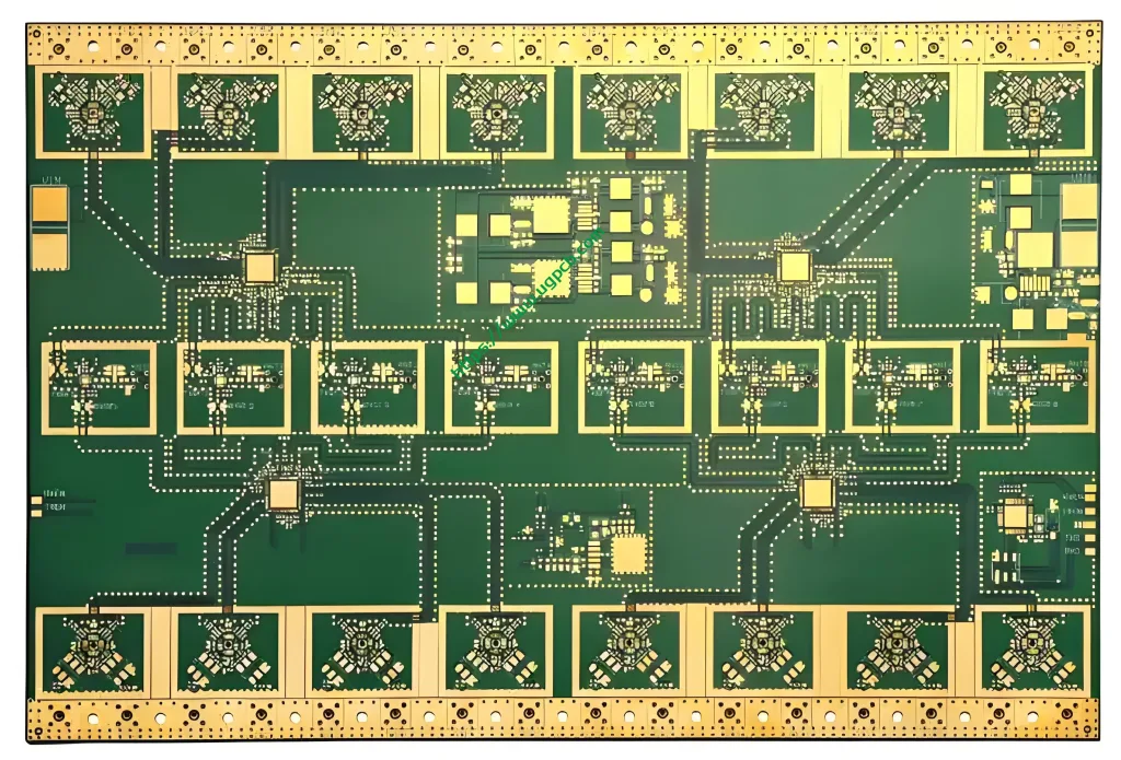
This product is an 8-layer high-frequency PCB manufactured using a “Rogers RO4350B Laminates and FR4 Hybrid Lamination” 프로세스. This innovative Hybrid Construction PCB strategically combines high-performance ceramic-filled PTFE material (RO4350B) with cost-effective FR4. The RO4350B material is used in critical signal layers to ensure exceptional high-frequency performance, while FR4 is used in inner power and ground layers for optimal cost-efficiency. This Mixed Dielectric PCB 설계 represents an intelligent choice for balancing performance and budget.

2. 중요한 설계 고려 사항
-
정밀한 임피던스 제어: 그만큼 RO4350B material offers a stable and low 유전 상수 (Dk=3.48). Combined with precision manufacturing processes, it enables highly accurate impedance control (typically ±5% or better), ensuring signal integrity for high-speed transmission.
-
Hybrid Stack-up Design: The design must clearly separate high-frequency signal layers (using RO4350B dielectric) from power/ground planes (which may use FR4). Rational stack-up planning is key to leveraging the benefits of hybrid material PCBs and controlling costs.
-
Low-Loss Design: The inherently low dissipation factor (Df) of RO4350B is foundational. Designers should also employ appropriate trace width, copper weight, and smooth copper foil surfaces (like reversed foil) to further minimize insertion loss.
-
열 관리: Although the 열전도도 (0.69W/m.K) of RO4350B is superior to most standard FR4, high-power applications still require careful thermal management through proper layout, thermal vias, and potential additional heat sinking.
3. 작동 방식 & 주요 특징
작동 원리
고주파에서 (typically above 500MHz), skin effect is significant, and signal integrity is highly susceptible to the dielectric properties of the substrate. The RO4350B ceramic hybrid High Frequency Circuit Board minimizes signal energy loss (삽입 손실) and phase distortion during transmission through its stable dielectric constant and very low loss tangent, ensuring low-noise, 고 충실도 신호 전송.
주요 특징 & 성능
-
Superior High-Frequency Stability: Stable Dk value across frequency and temperature variations ensures consistent and reliable circuit performance.
-
Exceptionally Low Signal Loss: Optimized for high-frequency applications, it significantly reduces signal attenuation, improving system SNR and transmission range.
-
Excellent Mechanical & 열 신뢰성: Glass-reinforced for high rigidity; resistant to high temperatures with a CTE matched to copper, enhancing long-term reliability.
-
Effective Heat Dissipation: A thermal conductivity of 0.69W/m.K aids in dissipating heat from high-power components, ensuring system stability.
-
Compliance with Safety Standards: The laminate meets the stringent UL 94V-0 가연성 등급.
-
안정적인 표면 마감: 이머젼 골드 (동의하다) treatment provides a flat soldering surface, 우수한 내산화성, and good contact conductivity, suitable for high-frequency signal connections and fine-pitch component soldering.
4. 재료 & 구조
-
주요 재료: 로저스 RO4350B (ceramic-filled PTFE composite) and FR-4 epoxy glass laminate.
-
전도성 층: 1온스 (35μm) Electrolytic Copper Foil.
-
표면 마감: 무전해 니켈 침지 금 (동의하다).
-
완성된 보드 두께: 2.5mm (± 10%).
-
유전체 두께: 0.338mm (전형적인, varies based on specific lamination structure).
-
Board Structure: 8-layer board. A typical stack-up involves a symmetrical or asymmetrical combination like [FR4-PP-RO4350B Core-RO4350B Core-PP-FR4], determined by electrical design requirements.
5. 과학적 분류
-
재료 유형별: Ceramic-Filled PTFE Hybrid Dielectric High-Frequency PCB / Composite Dielectric Substrate PCB.
-
By Application Frequency: RF 마이크로파 PCB / High-Frequency High-Speed PCB.
-
구조 별 & 프로세스: Multilayer Hybrid Laminate PCB / 8-Layer Precision Controlled Impedance Board.
6. Key Control Points in Production Flow
UGPCB possesses mature manufacturing processes for High Frequency Printed Circuit Boards. Critical control points include:
-
정밀 라미네이션: Strict control of lamination parameters (압력, 온도, 시간) for RO4350B and FR4 to prevent delamination/voids and maintain consistent dielectric thickness.
-
Fine-Line Etching: Utilization of high-precision imaging transfer technology to ensure trace edge smoothness and dimensional accuracy.
-
Stringent Impedance Control: End-to-end monitoring from design simulation to production, using advanced testing equipment (예를 들어, tdr) ~을 위한 100% sampling or full inspection.
-
Low-Loss Surface Treatment: Optimized ENIG process to ensure uniform plating, controlled thickness, and avoidance of issues like “블랙 니켈” that degrade high-frequency performance.
7. 기본 응용 프로그램 & 사용 사례
This product is designed for fields with stringent requirements for signal frequency and integrity, serving as a core component in High-Frequency Communication Equipment.
-
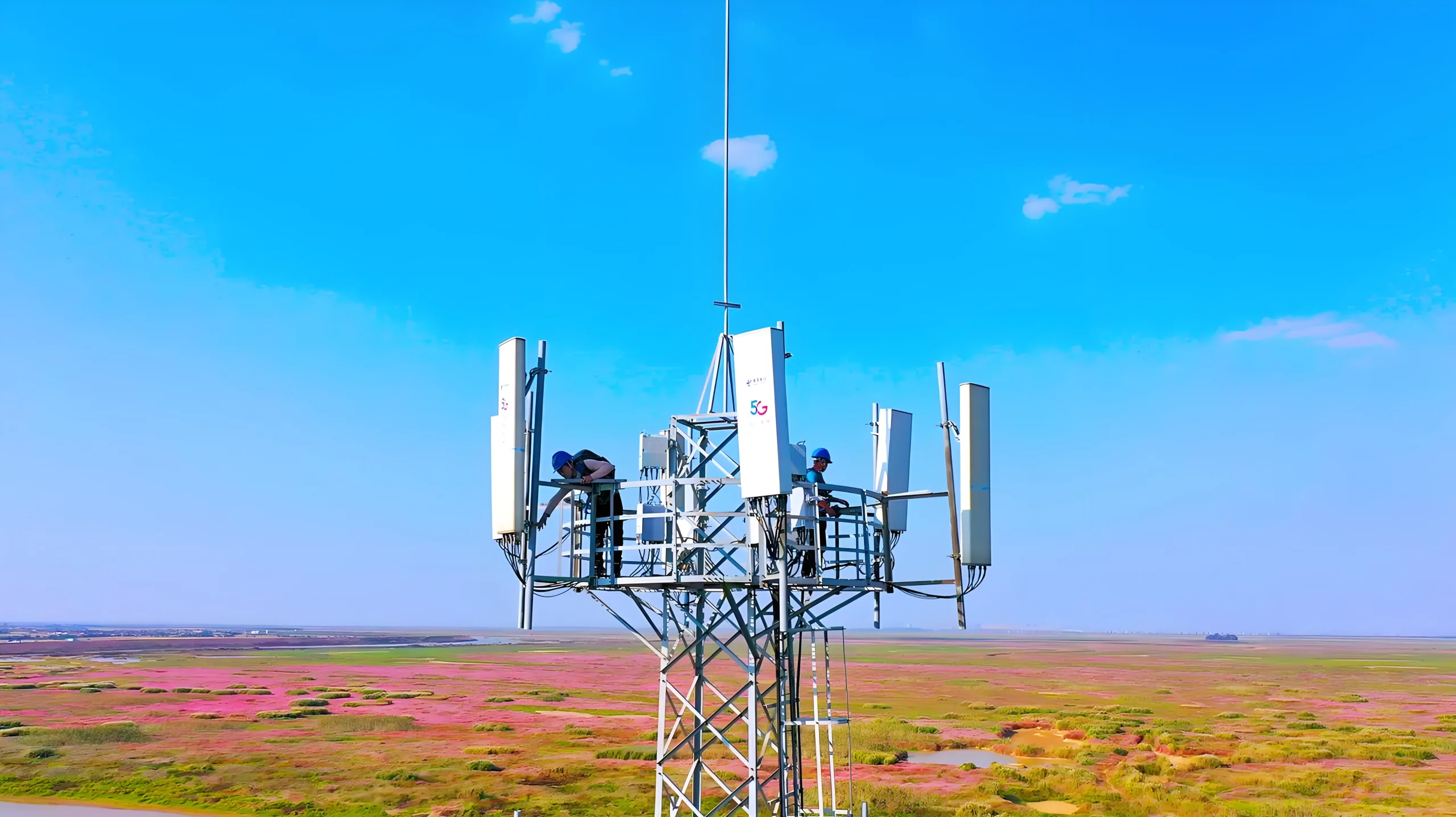
Communication Base Stations: 5G/4G Base Station RF power amplifiers, 안테나, 필터, 듀플렉서.
-
위성통신 & 레이더 시스템: Satellite receivers, radar transceiver modules, 내비게이션 시스템.
-
시험 & 측정 장비: 네트워크 분석기, 스펙트럼 분석기, high-frequency signal sources.
-
자동차 전자: 77GHz 밀리미터파 레이더, 고급 운전자 지원 시스템 (ADAS).
-
무선 인프라: Point-to-point microwave links, wireless access equipment.
Get Your High-Frequency PCB Solution Now
Your next-generation high-performance communication instrument deserves a more reliable core. UGPCB’s RO4350B Ceramic Hybrid 고주파 보드 is ready to power your lead in the signal age.
Click to contact our High-Frequency PCB experts for a free design consultation and an instant quote!
(This section should integrate a call-to-action button or contact form.)


Hi! I could have sworn I’ve been to this blog before but after checking through some
of the post I realized it’s new to me. Anyhow, I’m definitely delighted I found it and I’ll
be book-marking and checking back often!