What is a BGA PCB?
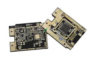
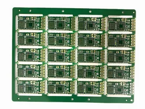
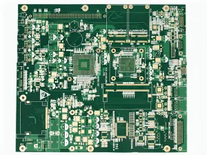
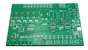
A Ball Grid Array (BGA) 인쇄 회로 기판 (PCB) is a type of 회로 기판 that features a grid of solder balls on its underside, used for connecting 전자 구성 요소 to the board. This design allows for higher input/output connection density and improved electrical performance compared to traditional through-hole or surface-mount technology (SMT) PCB.
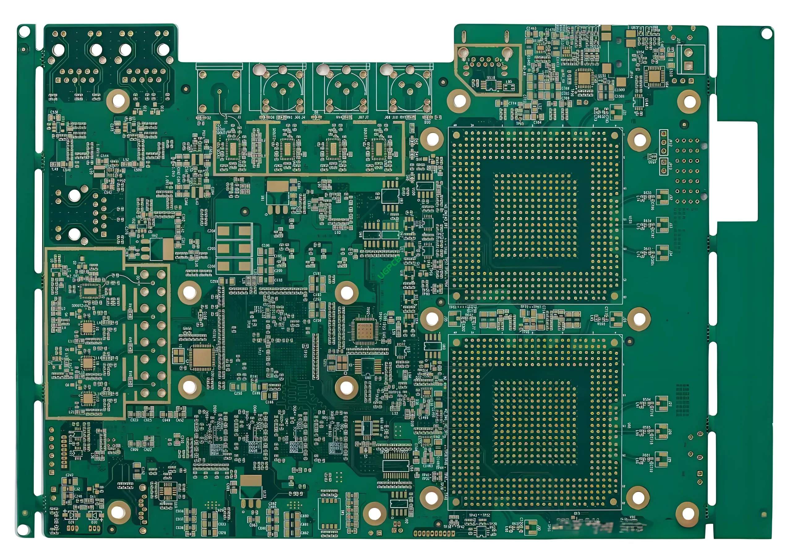
설계 요구 사항
Designing a BGA PCB involves several key considerations:
- 재료: Typically made from FR-4, 우수한 전기적 특성과 경제성으로 알려진 복합재료.
- 레이어 수: Multilayer designs are common, providing more space for complex circuitry.
- 구리 두께: Generally specified as 1/1OZ, balancing conductivity with cost-effectiveness.
- 표면 처리: Often includes immersion gold to enhance solderability and protect against oxidation.
- 추적과 공간: Minimum trace and space are typically set at 4mil, 회로 설계의 미세한 세부 사항 허용.
어떻게 작동하나요??
The BGA PCB functions by providing a platform where electronic components can be mounted and interconnected using a grid of solder balls. These balls are aligned in a pattern on the underside of the board, corresponding to contact pads on the component. When heat is applied, the solder melts and creates a strong bond, ensuring reliable electrical connections.
응용
Due to their high density and reliability, BGA PCBs are widely used in various electronic products including:
- Computer motherboards
- High-performance servers
- 네트워킹 장비
- Advanced consumer electronics like gaming consoles and smart devices
분류
BGA PCBs can be classified based on several factors:
- 재료로: 비용 균형으로 인해 가장 일반적으로 FR-4로 만들어집니다., 힘, 및 전기 특성.
- 레이어 수에 의해: Can range from double-sided to multilayer configurations, 회로의 복잡성에 따라.
- 표면 처리에 의한: 옵션에는 침수 금이 포함됩니다., hasl, or organic solderability preservatives (OSP), 각각은 서로 다른 수준의 보호 및 납땜성을 제공합니다..
사용된 재료
기본 재료 used in manufacturing BGA PCBs include:
- FR-4: 우수한 기계적 강도와 열적 안정성을 제공하는 유리 강화 에폭시 적층판.
- 구리: 전도층에 사용, 설계 요구 사항에 따라 두께가 다양함.
- 솔더 마스크: 일반적으로 녹색 또는 흰색, 산화 및 우발적인 단락으로부터 구리 트레이스를 보호합니다..
- 이머젼 골드: A surface treatment that improves solderability and protects against corrosion.
성능 특성
Key performance attributes of a BGA PCB include:
- 고밀도: Allows for more components to be packed into a smaller area.
- 신뢰할 수 있음: The use of solder balls reduces the risk of mechanical failure due to vibration or impact.
- 신호 무결성: 더 짧은 신호 경로와 감소된 누화로 인해 개선됨.
구조적 구성
구조적으로, a BGA PCB comprises:
- 전도성 층: 구리로 만든, 원하는 회로 패턴으로 에칭.
- 절연층: 전도성 층 사이의 전기적 단락 방지.
- 솔더볼: Arranged in a grid pattern on the underside of the board for component attachment.
독특한 특징
Some notable features of a BGA PCB are:
- 파인 피치: 고밀도 상호 연결 허용, 컴팩트한 장치에 이상적입니다..
- 견고성: The use of solder balls provides a strong mechanical bond between the board and components.
- 다재: 사용자 정의 가능한 레이어 수 및 재료 선택으로 인해 광범위한 응용 분야에 적합합니다..
생산 과정
The manufacturing process of a BGA PCB involves several steps:
- 디자인 및 레이아웃: 전문 소프트웨어를 사용하여 회로 패턴 생성.
- 재료 준비: 기본 재료를 크기에 맞게 절단하고 표면을 청소합니다..
- 라미네이션: 열과 압력을 가해 개별 레이어를 적층하고 접착.
- 에칭: 원하는 회로 경로를 형성하기 위해 과도한 구리를 제거합니다..
- 도금: 비아와 노출된 구리 영역에 얇은 금속층 추가.
- 솔더 마스크 적용: 흔적을 보호하기 위해 녹색 또는 흰색 코팅 적용.
- 표면 처리: Applying immersion gold or other treatments for solderability.
- 최종검사: 배송 전 품질과 기능성 보장.
사용 사례
Common scenarios where a BGA PCB might be employed include:
- 모바일 장치의 고밀도 상호 연결 애플리케이션.
- 낮은 신호 손실이 요구되는 고급 통신 시스템.
- 열악한 환경에서 안정적인 성능이 필요한 휴대용 의료 기기.
- 견고성과 수명을 요구하는 자동차 전자 장치.
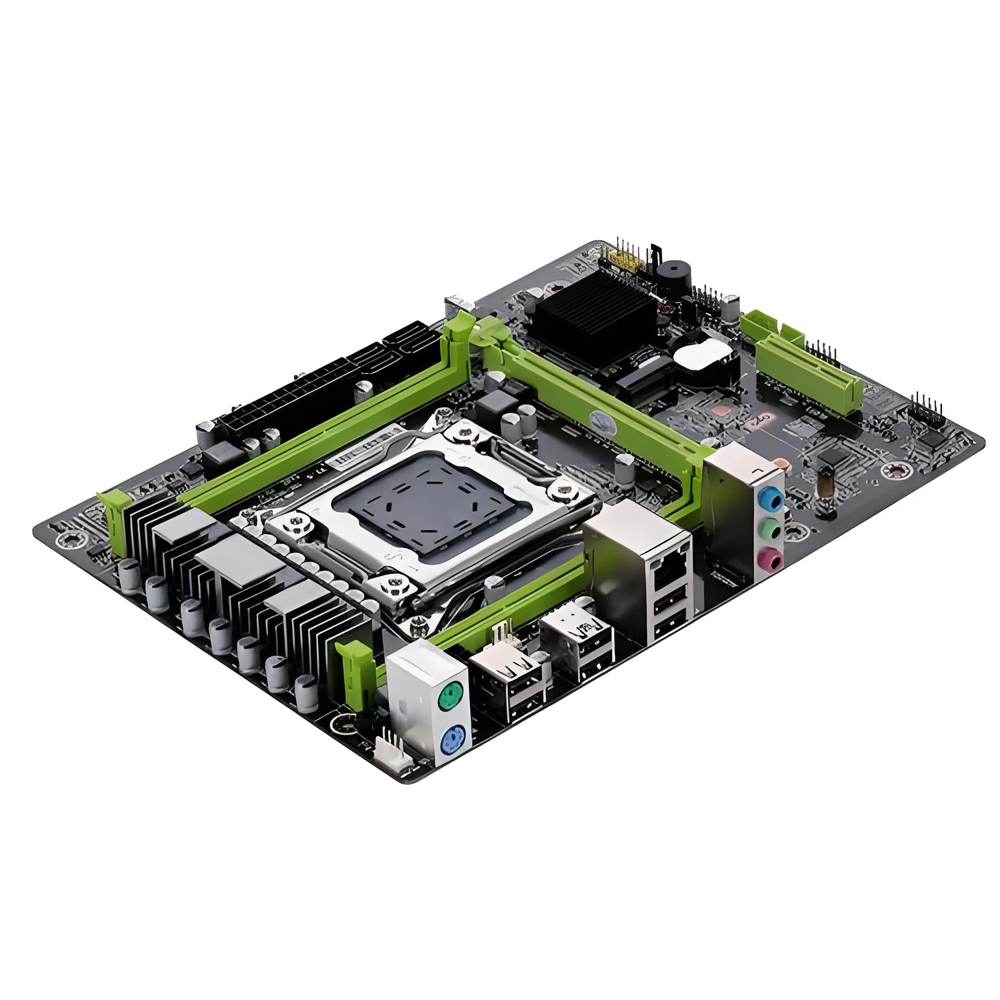
요약하면, the BGA PCB represents a significant advancement in printed circuit board technology, 현대 전자 애플리케이션에 비교할 수 없는 복잡성과 성능을 제공합니다.. Its design flexibility, combined with superior signal integrity and durability, makes it an essential component in the development of next-generation electronic products and beyond