

1. 제품개요
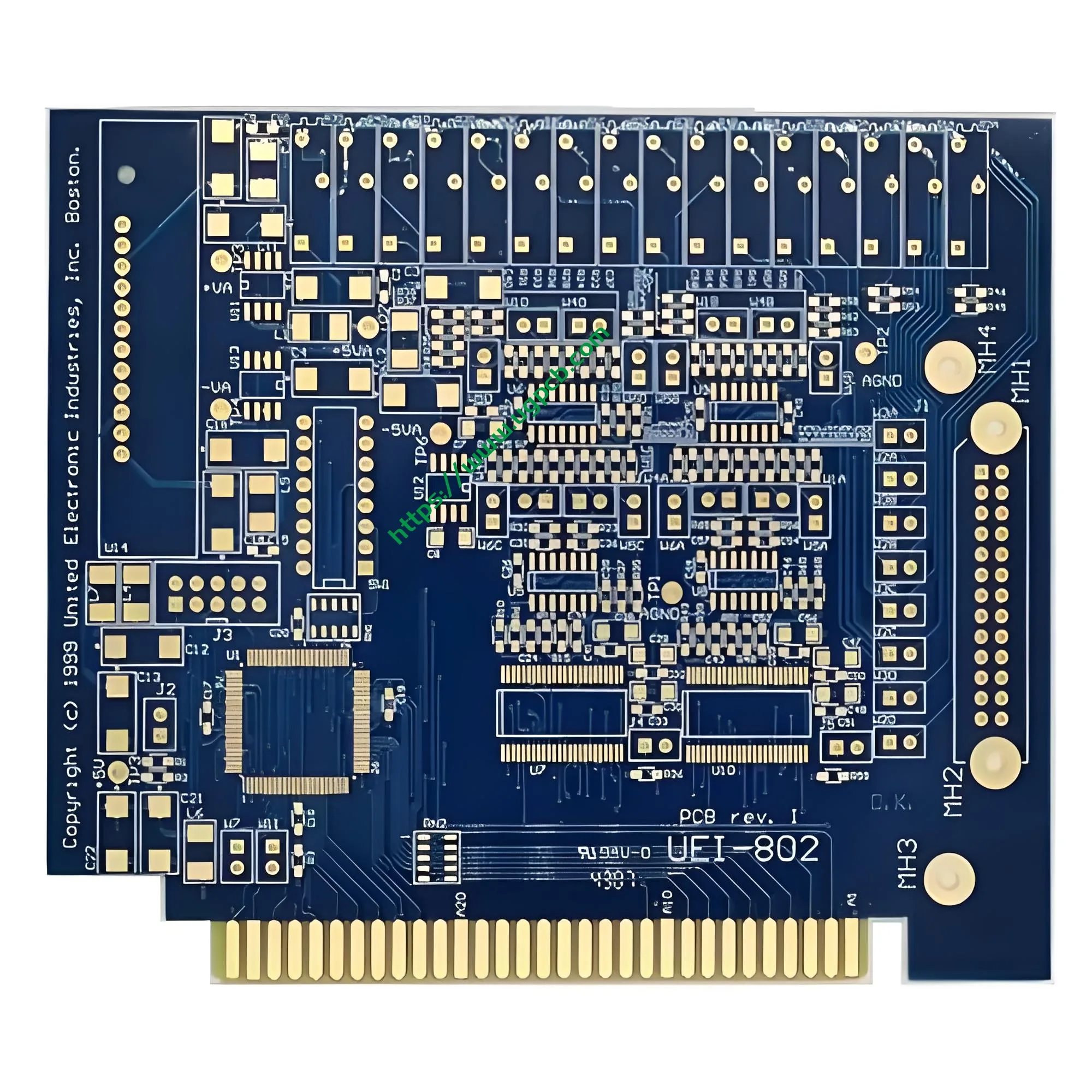
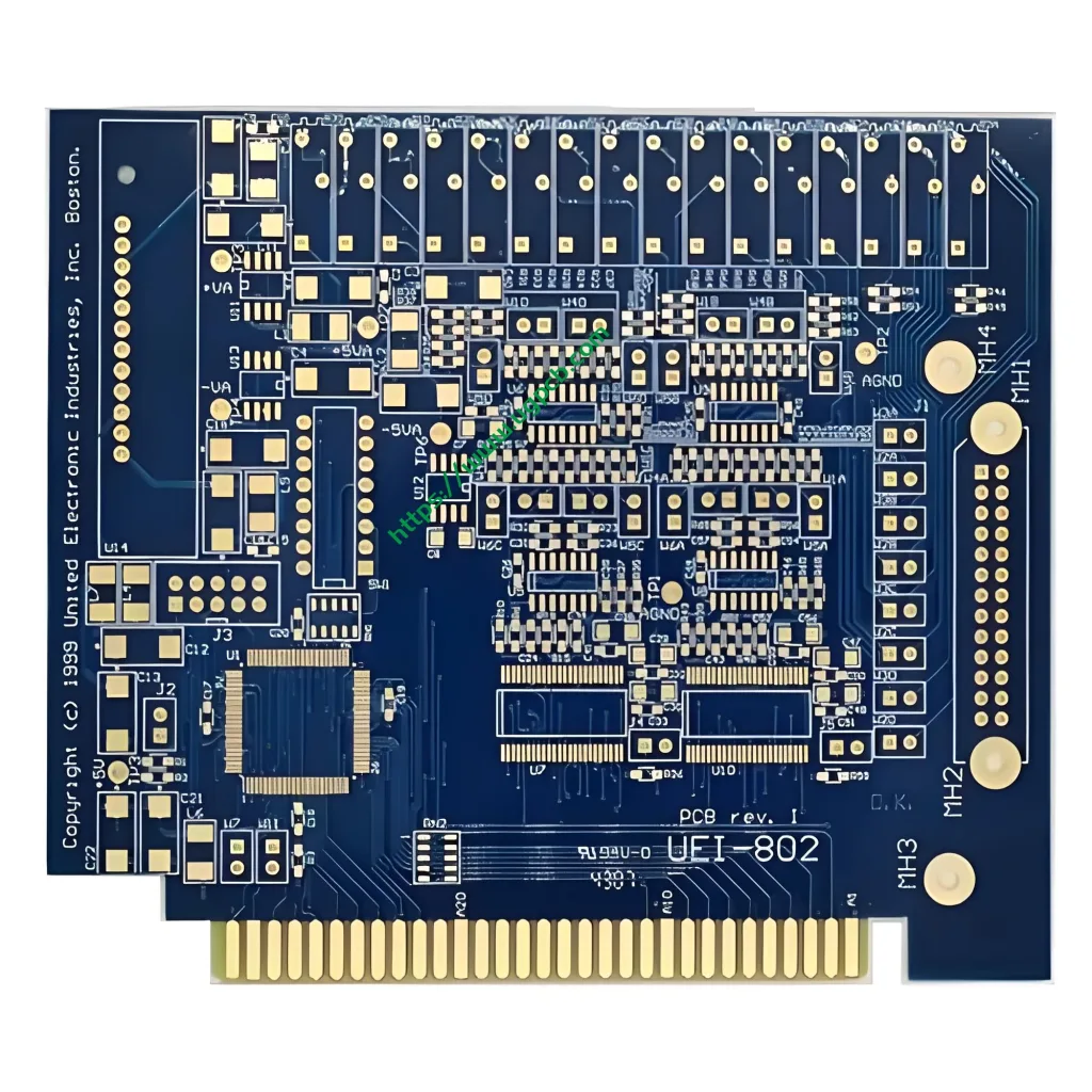
A double‑sided gold finger 인쇄 회로 기판 (PCB) features gold‑plated contacts – commonly called “gold fingers” – arranged along the board edge. These contacts create a pluggable electrical path when inserted into a mating connector, such as a card slot or socket. All signals and power flow through these finger‑shaped terminals.
UGPCB’s double‑sided gold finger PCB uses an FR4 substrate with a 2‑layer design. 보드 두께는 1.6 mm, and both inner and outer layers have 1 온스 구리. The minimum drilled via diameter is 0.3 mm, and the trace width and spacing are both 0.15 mm. The surface finish is immersion gold (동의하다) over the entire board, with additional electroplated hard gold selectively applied to the gold finger areas. This product offers the routing flexibility of a double‑sided board together with the proven reliability of gold finger connections. It serves a wide range of electronic systems that require board‑to‑board plug‑in interfaces.
2. Product Classification and Positioning
According to IPC‑6012 (the rigid printed board qualification and performance specification), 이 제품은 다음 카테고리에 속합니다:
| 분류 차원 | 범주 |
|---|---|
| 구조 별 | Double‑sided PCB – conductive traces on both sides |
| By Interconnection Method | With plated‑through holes (PTH) |
| By IPC‑6012 Performance Class | 수업 2 (전용 서비스 전자 제품) – suitable for most gold finger applications |
| 기판 재료별 | FR4 rigid laminate (S1141 grade) |
| 표면 마감별 | 동의하다 (electroless nickel / 침수 금) + selective electroplated hard gold on gold fingers |
| By Function | Gold finger PCB / 에지 커넥터 PCB |
This product is positioned as amedium‑to‑high‑reliability plug‑in connection 해결책. It combines the design freedom of double‑sided routing with the signal integrity of gold finger edge connectors.
3. 주요 기술 매개변수
3.1 기판: FR4 + S1141 Laminate
FR4 is the most common rigid substrate in the PCB industry. It consists of glass‑fiber‑reinforced epoxy resin, which provides excellent mechanical strength, 전기 절연, 및 내열성. 이 제품은 S1141 FR4 laminate from Shengyi Technology, which complies with IPC‑4101/21.
Key performance indicators for S1141 (tested on 1.6 mm specimens) 아래에 나열되어 있습니다.
| 매개 변수 | 전형적인 가치 | 테스트 방법 |
|---|---|---|
| 유리전이온도 (Tg) | 140℃ (DSC) | IPC‑TM‑650 2.4.25 |
| 열분해 온도 (Td) | 310℃ (5 % 체중 감량) | IPC‑TM‑650 2.4.24.6 |
| Z축 CTE (Tg 이전) | 65 ppm/°C | IPC‑TM‑650 2.4.24 |
| Z축 CTE (after Tg) | 300 ppm/°C | IPC‑TM‑650 2.4.24 |
| 유전 상수 (DK, 1 MHz) | 4.6 | IPC‑TM‑650 2.5.5.9 |
| 소산 인자 (Df, 1 MHz) | 0.015 | IPC‑TM‑650 2.5.5.9 |
| 가연성 등급 | UL 94 V-0 | UL 94 |
| 수분 흡수 | 0.15 % | IPC‑TM‑650 2.6.2.1 |
데이터 소스: Shengyi S1141 Technical Data Sheet, compliant with IPC‑4101/21.
UL 94 V-0 is the highest flame‑retardant rating in the UL 94 vertical burn test. It requires that after two 10‑second flame applications, the total flaming combustion time for each specimen does not exceed 10 초, and no flaming drips ignite the cotton indicator. This ensures the PCB remains safe under abnormal heating or short‑circuit conditions.

3.2 보드 두께: 1.6 mm
그만큼 1.6 mm thickness is the industry standard for rigid PCBs. It also serves as the baseline thickness for S1141 material property data. This thickness achieves an optimal balance between mechanical strength, insertion stability, 그리고 제조비용. It is widely compatible with standard connector slots.
3.3 구리 두께: 1 온스 (약 35 μm)
Both inner and outer layer copper foils are1 온스 (온스) , which is approximately 35 μm 두께. According to IPC‑6012, the minimum finished copper thickness for Class 1 그리고 수업 2 boards is 48 μm. Starting with 1 oz foil ensures that the final thickness after processing meets these requirements. This copper weight supports adequate current‑carrying capacity (approximately 4‑6 A, depending on trace width) while preserving fine‑line etching precision. The trace width and spacing of 0.15 mm (~에 대한 6 밀) are reliably producible with 1 온스 구리.
3.4 Minimum Via Diameter: 0.3 mm
The minimum mechanical drilled hole diameter is 0.3 mm, which is well within standard through‑hole technology capability. This supports plated‑through‑hole (PTH) processing to ensure reliable electrical interconnection between layers. IPC‑6012용, all PTHs must pass thermal stress testing (288 °C solder dip) to verify structural integrity.
3.5 추적 너비와 간격: 0.15 mm / 0.15 mm
A trace width of 0.15 mm (약 6 밀) and a spacing of 0.15 mm represent a fine‑line capability within conventional PCB manufacturing. ~에 1 오즈 구리 두께, 에이 0.15 mm trace can carry approximately 0.5‑0.8 A of current based on IPC‑2221 calculations. This meets the needs of most signal transmission and low‑power supply applications. This combination of width and spacing ensures reliability while keeping manufacturing costs under control.
4. 표면 마감: Immersion Gold plus Electroplated Gold Fingers
이 제품은combined surface finish process: 침수 금 (동의하다) across the entire board, ~와 함께electroplated hard gold selectively applied to the gold finger areas. This is the standard and optimal process for gold finger PCBs.
4.1 이머젼 골드 (동의하다) 프로세스
무전해니켈 / 이머젼 골드 (동의하다) is a finish where nickel is first chemically deposited onto the copper surface, followed by a thin gold layer deposited through a displacement reaction.
당IPC‑4552 Revision A (issued 2017) :
- 니켈 두께: 3 μm ~ 6 μm (120 μin to 240 μin)
- 금 두께: 0.04 μm ~ 0.10 μm (1.6 μin to 4.0 μin)
- Recommended gold thickness: 0.04 μm ~ 0.07 μm (1.6 μin to 2.8 μin)
데이터 소스: IPC‑4552 – Performance Specification for Electroless Nickel / 이머젼 골드 (동의하다) 인쇄 기판용 도금.
Advantages of ENIG:
- Flat surface suitable for fine‑pitch traces and BGA packages
- Excellent solderability supporting lead‑free soldering (예를 들어, SAC305)
- Strong oxidation resistance with long shelf life
- Thin gold layer keeps costs manageable
4.2 Electroplated Gold Fingers – The Key Feature
The gold finger areas receiveadditional electroplated hard gold. Unlike the soft gold used in ENIG, electroplated hard gold contains hardeners such as cobalt or nickel (gold‑cobalt or gold‑nickel alloy). Its hardness can exceed HV 200, providing far greater wear resistance than soft gold.
Why must gold fingers use electroplated hard gold?
ENIG gold is extremely thin (only 0.04‑0.10 μm) and soft (hardness below HV 90). It wears away after just 3‑5 insertion cycles. 전기 도금된 하드 골드, with a thickness typically above 0.76 μm, can withstand hundreds or even thousands of insertion cycles.
당IPC‑4556 (Hard Gold Performance Specification) :
| 응용클래스 | Minimum Gold Thickness | 일반적인 응용 프로그램 |
|---|---|---|
| 수업 2 (튼튼한) | ≥ 0.76 μm (30 μin) | Most gold finger applications |
| 수업 3 (높은 신뢰성) | ≥ 1.27 μm (50 μin) | High‑cycle insertion, 산업의 / 군대 |
| Nickel Underlayer | 3‑5 μm | Required for all hard gold deposits |
데이터 소스: IPC‑4556 – Performance Specification for Electroplated Hard Gold for Connectors and Gold Fingers.
The electroplated gold finger process used in this product complies with IPC‑4556 Class 2 through Class 3 표준, ensuring insertion life and contact reliability.
5. 디자인 고려 사항
5.1 Gold Finger Chamfering
The insertion end of the gold fingers must bechamfered to enable smooth entry into the connector slot.
- Chamfer angle: Typically 30° or 45°
- Chamfer depth: 을 위한 1.6 mm 보드 두께, the chamfer depth is typically 0.8‑1.0 mm, leaving a 0.6‑0.8 mm blunt edge at the tip
- Remaining tip thickness: Approximately one‑third to one‑half of the original board thickness
- Critical requirement: No solder mask may cover the chamfered area, and the gold layer must fully cover the chamfered bevel
5.2 Gold Finger Area Design Rules
- Gold fingers should be placed at the board edge in an orderly array
- Minimum spacing between adjacent gold fingers should be ≥ 7 밀 (약 0.178 mm)
- The gold finger area must be clearly marked in the Gerber files with explicit plating instructions
5.3 Impedance Control Considerations
FR4 material has a dielectric constant Dk = 4.6 ~에 1 MHz. 을 위한 50 Ω single‑ended or 100 Ω differential impedance control, designers can adjust trace width and dielectric thickness. 그만큼 0.15 mm trace width and spacing in this product meet most signal integrity requirements for standard designs.
6. 작동 원리
A double‑sided gold finger PCB operates through two core mechanisms: electrical contact 그리고신호 전송.
- Electrical connection: The gold finger contacts at the board edge physically mate with the metal spring contacts inside the connector slot, establishing a low‑resistance electrical path.
- 신호 전송: The PCB traces route signals from various 구성 요소 (작은 조각, 저항기, 커패시터, 등.) to the gold finger contacts, which then transmit through the connector to the motherboard or backplane. The double‑sided design allows routing on both the top and bottom layers, significantly increasing routing density and design flexibility.
- Pluggability: The electroplated hard gold layer on the gold fingers provides sufficient wear resistance to support multiple insertion cycles without degrading contact resistance or signal integrity.
7. 애플리케이션 및 사용 사례
Double‑sided gold finger PCBs are widely used in electronic devices that requirepluggable connections. 일반적인 응용 프로그램은 다음과 같습니다:
| 적용분야 | 특정 제품 |
|---|---|
| 컴퓨팅 & 서버 | 메모리 모듈 (DDR, DDR2, DDR3, DDR4, Dr5), 그래픽 카드, network interface cards, 확장 카드 |
| 가전제품 | USB 드라이브, memory cards, 카드 독자, 스마트폰, 스마트워치 |
| Communications Equipment | 라우터, 스위치, 통신 모듈 |
| 산업 제어 | Industrial control boards, data acquisition cards, 테스트 설비 |
| 자동차 전자 | In‑vehicle control units, 인포테인먼트 시스템 |
| 의료 기기 | Medical electronic modules (with IPC‑6012EM medical supplement) |
| 항공우주 | Avionics modules (with IPC‑6012FS aerospace supplement) |
FR4 double‑sided gold finger PCBs are particularly suitable formedium‑complexity, cost‑sensitive applications that demand plug‑in connectivity.
8. 제조 공정 흐름
UGPCB follows a standard production sequence for double‑sided gold finger PCBs:
- 절단 – Cut FR4 copper‑clad laminate to working panel dimensions.
- 교련 – Drill 0.3 mm through‑holes and mounting holes.
- PTH / 패널 도금 – Apply electroless copper deposition in holes, then panel plate.
- 패턴 전송 – Expose and develop the circuit pattern.
- 패턴 도금 – Electrolytically plate circuits and holes to 1 온스 구리.
- 에칭 – Remove unprotected copper foil to form the final circuit traces.
- 솔더 마스크 – Apply green or other coloured solder mask ink.
- 표면 마감 – ENIG – Apply electroless nickel and immersion gold over the entire board.
- Gold Finger Plating – Selectively electroplate hard gold on the gold finger areas.
- Gold Finger Chamfering – Chamfer the insertion end.
- 전기 테스트 – Perform flying‑probe or fixture testing.
- 육안검사 – Inspect per IPC‑A‑600.
- 포장 & 해운 – Vacuum‑pack for moisture protection.
9. Performance and Quality Standards
This product is designed and manufactured in strict compliance with the following international standards:
| 기준 | 제목 | 범위 |
|---|---|---|
| IPC‑6012 | 경질 인쇄 기판의 자격 및 성능 사양 | Overall performance and reliability |
| IPC‑A‑600 | 인쇄 기판의 수용성 | Visual appearance and acceptance criteria |
| IPC‑4552 | ENIG Performance Specification | Immersion gold process control |
| IPC‑4556 | Electroplated Hard Gold Performance Specification | Gold finger hard gold process |
| IPC‑4101/21 | Specification for Rigid and Multilayer Printed Board Substrate Materials | FR4 material specifications |
| UL 94 V-0 | Standard for Safety – Flammability of Plastic Materials | Flame‑retardant certification |
10. UGPCB를 선택하는 이유는 무엇입니까??
- Professional gold finger manufacturing experience – UGPCB has mature capabilities in electroplating and chamfering.
- End‑to‑end quality control – Every step from cutting to final inspection is managed per IPC standards.
- Traceable materials – Uses brand‑name FR4 laminates such as Shengyi S1141 with clear source traceability.
- Fast delivery – A dedicated double‑sided PCB production line supports rapid prototyping and volume production.
- 기술지원 – Provides DFM (제조 가능성을위한 설계) reviews and impedance control recommendations.
11. Inquire Now
UGPCB is committed to delivering high‑value double‑sided gold finger PCB solutions to customers worldwide. 당신이 필요 여부샘플 프로토타이핑, small‑batch trial production, or high‑volume manufacturing, we have the expertise to serve you.
Contact us for a quote:
- Provide Gerber files or PCB 설계 데이터
- Specify gold finger plating thickness (0.76 μm ~ 1.27 μm recommended)
- Confirm chamfer angle (30° 또는 45°) and any other special requirements
데이터 소스 선언
The technical data and standard references in this document are sourced from: IPC‑6012 Qualification and Performance Specification for Rigid Printed Boards; IPC‑4552 Performance Specification for Electroless Nickel / 이머젼 골드 (동의하다) 인쇄 기판용 도금; IPC‑4556 Performance Specification for Electroplated Hard Gold for Connectors and Gold Fingers; IPC‑A‑600 Acceptability of Printed Boards; UL 94 Standard for Safety – Flammability of Plastic Materials; and the Shengyi S1141 Technical Data Sheet (compliant with IPC‑4101/21).













