


나. 제품개요
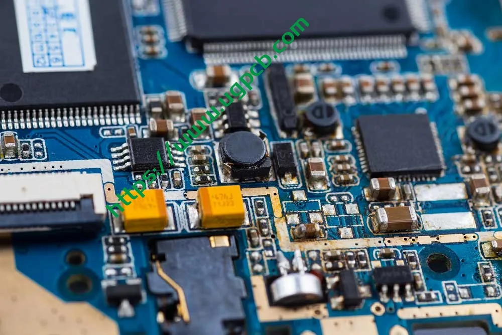
UGPCB 양면 스루홀 PCB 보드는 고성능 2레이어 리지드입니다. 인쇄 회로 기판 도금된 스루홀을 사용하여 FR-4 유리-에폭시 기판 위에 제작됨 (PTH) 기술. 이사회에서 측정 86.9 × 73.58 mm 두께의 1.0 mm, 동박 두께 1/1 온스 (35 외부 및 내부 레이어 모두에서 μm), 무연 열풍 솔더 레벨링 (HASL) 표면 마감. 솔더 마스크는 녹색입니다., 그리고 실크스크린의 전설은 흰색이다.
양면 스루홀 PCB (양면 인쇄 회로 기판) 절연 기판의 양면에 전도성 회로가 있음, 두 층 사이의 전기적 상호 연결을 가능하게 하는 도금된 관통 구멍 포함. 단면 PCB와 비교, double-sided PCBs offer 60%–80% higher routing density and support more complex circuit designs. UGPCB, ISO 인증 품질 시스템과 IPC 준수 제조 프로세스로 뒷받침됩니다., 고품질 양면 스루홀 PCB 및 턴키 제공 PCB 전 세계 전자 제조업체에 대한 서비스.
II. 제품 정의 및 기술 사양
IPC-6012F에 따라 경질 인쇄 기판의 자격 및 성능 사양 (9월 출판 2023), 양면 스루홀 PCB는 도금된 스루홀이 있는 견고한 인쇄 기판으로 분류됩니다. (유형 2). 핵심 특징은 구리 도금 홀 벽을 통해 양쪽 도체 사이의 전기적 연결입니다.. UGPCB는 IPC-6012F를 완벽하게 준수하여 이 제품을 제조하고 클래스를 충족합니다. 2 성능 요구 사항 (전용 서비스 전자 장비).
주요 사양:
| 매개 변수 | 사양 |
|---|---|
| 기판 재료 | FR-4 (난연 UL 94 다섯-0) |
| 레이어 수 | 2 레이어 (양면) |
| 보드 두께 | 1.0 mm |
| 보드 크기 | 86.9 × 73.58 mm |
| 최소 구멍 직경 | 0.236 mm |
| 최소 선 너비 / 간격 | 0.32 × 0.37 mm |
| 동박 두께 | 1/1 온스 (대략. 35 각 변의 μm) |
| 표면 마감 | 무연 HASL (열기 솔더 레벨링) |
| 솔더 마스크 / 전설 | 녹색 솔더 마스크 / 흰색 실크스크린 |
III. 설계 지침
3.1 기판 재료 선택 - FR-4의 엔지니어링 가치
FR-4 미국전기제조협회(National Electrical Manufacturer Association)가 정한 난연성 등급 지정입니다. (아니요). 편지 “정말로” 난연성을 상징하는 스탠드, 그리고 숫자 “4” 직조된 유리섬유로 강화된 에폭시 수지 시스템을 나타냅니다.. IPC-4101의 경우 경질 및 다층 인쇄 기판용 기본 재료 사양, FR-4 등급 A1은 최적의 기계적 강도를 갖춘 핵심 성능 계층을 나타냅니다., 전기적 특성, 장기적인 신뢰성.
FR-4의 핵심 성과 지표 (원천: IPC-4101 및 산업 표준):
-
유리전이온도 (Tg): 130-140°C (표준 FR-4)
-
유전 상수 (DK) @ 1 GHz: 4.2–4.5
-
소산 인자 (Df) @ 1 GHz: ≤ 0.020
-
가연성 등급: UL 94 다섯-0
-
수분 흡수 (24 시간): ≤ 0.10%
FR-4는 뛰어난 기계적 강도 균형을 제공하기 때문에 PCB 업계에서 여전히 주요 기판 소재로 남아 있습니다., 전기 절연, 치수 안정성, 및 가공성.
3.2 IPC-2221에 따른 회로 설계 표준
IPC-2221의 경우 인쇄 기판 설계에 대한 일반 표준, 도체 폭 설계는 전류 전달 용량을 고려해야 합니다., 온도 상승, 그리고 구리 두께. IPC-2221 전류 전달 용량 공식은 다음과 같습니다.:
I = k · ΔT^0.44 · A^0.725
어디:
-
I = 최대 전류 전달 용량 (에이)
-
k = 경험적 상수 (0.048 외부 레이어용, 0.024 내부 레이어용)
-
ΔT = 허용 온도 상승 (℃)
-
A = 도체 단면적 (밀²), 여기서 A = W × T
UGPCB 제품의 선폭은 0.32 mm (대략. 12.6 밀), 줄 간격 0.37 mm (대략. 14.6 밀), 구리 두께 1 온스 (35 μm). 10°C 온도 상승이 있는 외부 레이어 트레이스의 경우:
A = 0.32 mm × 0.035 mm = 0.0112 mm² ≒ 17.36 밀²
나 = 0.048 × 10^0.44 × 17.36^0.725 ≒ 0.048 × 2.75 × 7.82 ≈ 1.03 에이
이 도체 폭은 대략적으로 지원됩니다. 1 현재의 A, 대부분의 가전 제품 및 산업 제어 장비의 전력 및 신호 전송 요구 사항을 충족합니다.. IPC-2221에서는 PCB 서비스 수명을 보존하기 위해 최대 온도 상승을 10°C 또는 20°C로 제한할 것을 권장합니다..
3.3 구멍 직경 및 종횡비 설계
스루홀의 종횡비는 드릴링 및 홀 금속화 난이도를 평가하는 데 중요한 척도입니다.. 공식은:
종횡비 = 보드 두께 / 드릴 구멍 직경
UGPCB 제품의 경우 1.0 mm 보드 두께 및 0.236 mm 최소 구멍 직경:
종횡비 = 1.0 / 0.236 ≈ 4.24:1
이 종횡비는 업계에서 권장하는 상한보다 훨씬 낮습니다. 10:1 그리고 보수적인 설계 임계값은 8:1. 드릴링 및 금속화의 난이도가 낮음을 나타냅니다., 높은 수율, 통제된 비용, 스루홀 신뢰성 보장.
3.4 랜드 패턴 디자인 참고자료
IPC-7351의 경우 표면 실장 설계 및 랜드 패턴 표준에 대한 일반 요구 사항, 랜드 패턴 설계는 적절한 솔더 필렛 형성을 보장하고 납땜성을 충족해야 합니다., 검사 가능성, 및 재작업성 요구사항. 스루홀 부품용, 랜드 직경은 일반적으로 충분한 환형 링 폭을 확보하기 위해 홀 직경의 1.8~2.2배가 권장됩니다..
IV. 작동 원리
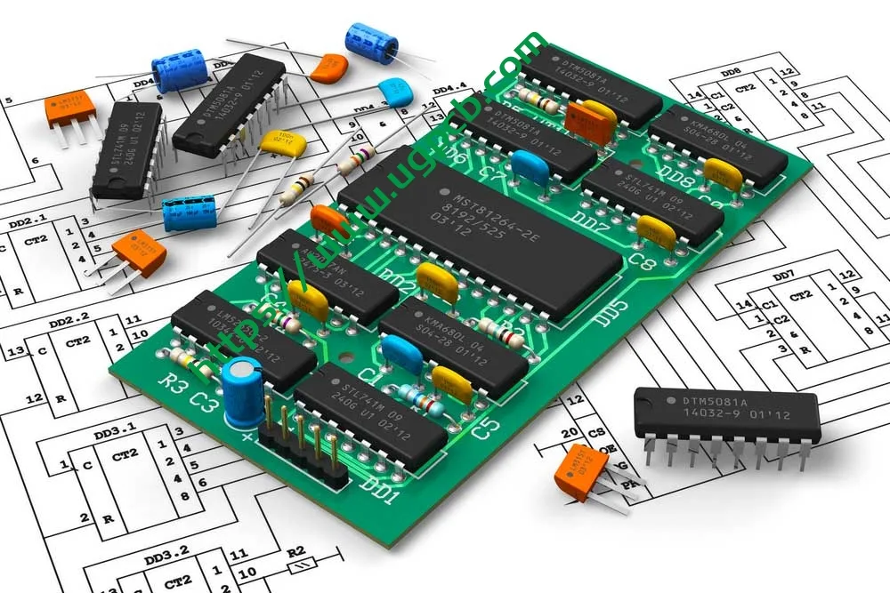
양면 스루홀 PCB는 세 가지 핵심 기술로 작동합니다.:
1. 양면 라우팅 — FR-4 절연 기판의 상하 양면에 전도성 회로 패턴이 에칭되어 있습니다., 양쪽에 부품 배치 가능. 이는 회로 밀도와 설계 유연성을 크게 향상시킵니다..
2. 도금 스루홀 (PTH) 상호 연결 — 드릴링 후, 무전해 구리 증착 및 전해 구리 도금은 홀 벽에 전도성 층을 형성합니다.. 이는 낮은 저항을 생성합니다., 상단과 하단 레이어 사이의 매우 안정적인 전기 연결. IPC-6012F 클래스에 따라 2, 구멍 벽의 최소 평균 도금 구리 두께는 ≥이어야 합니다. 20 μm.
3. 부품 조립 및 납땜 — 부품은 구멍을 통해 장착됩니다. (tht) 또는 표면 실장 (SMT) 리플로우 또는 웨이브 솔더링을 통해 전기적으로 연결되는 기술, 완전한 기능을 갖춘 PCBA 생산 (인쇄 회로 보드 어셈블리) 기준 치수.
다섯. 제품 분류
견고한 인쇄 기판에 대한 IPC-6012F 분류 시스템에 따라, UGPCB의 제품은 다음과 같이 분류됩니다.:
| 분류 차원 | 범주 |
|---|---|
| 건설 별 | 도금된 스루홀이 있는 견고한 인쇄 기판, 양면 (IPC-6012F 유형 2) |
| 성능 등급별 | 수업 2 (전용 서비스 전자 장비) |
| 기판 재료별 | FR-4 에폭시 유리 직물 라미네이트 (IPC-4101/21) |
| 레이어 수에 의해 | 2-레이어 보드 |
| 표면 마감별 | 무연 HASL |
| 가연성 등급별 | UL 94 다섯-0 |
애플리케이션 도메인별, 이 제품은 일반 산업용 양면 PCB 범주, 가전제품에 적합, 산업 제어, 통신 장비, 전원 어댑터, 및 기타 중간 신뢰성 애플리케이션.
VI. 재료 구성
6.1 기판 - FR-4 동박 적층판
FR-4는 강화재로 전자등급 직조 유리 직물과 바인더로 에폭시 수지로 구성된 유리 강화 에폭시 라미네이트입니다., 고온 및 고압 하에서 굳어짐. UL이다 94 다섯-0 가연성 등급은 수직 연소 시험에서, 물질은 내부에서 스스로 소화됩니다. 10 10초 동안 화염을 두 번 적용한 후 각각 몇 초 후에, 면화에 불을 붙이는 불타는 물방울이 없이.
6.2 구리 포일 — 1/1 온스
1온스 (1 온스) 구리박의 두께는 다음과 같습니다. 35 μm (1.37 밀). UGPCB 용도 1 두 외부 레이어 모두에 OZ 구리 (지정된 1/1 온스), 양쪽에서 동일한 전류 전달 용량과 전도성을 보장합니다..
6.3 표면 마감 - 무연 HASL
무연 HASL에는 용융된 무연 솔더에 PCB를 담그는 작업이 포함됩니다. (일반적으로 Sn-Cu, Sn-Cu-Ni, 또는 Sn-Ag-Cu 합금), 그런 다음 고압 열풍 칼을 사용하여 과도한 땜납을 수평으로 유지하고 제거합니다.. 이것은 유니폼을 생산합니다, 구리 표면에 납땜 가능한 보호 코팅. 이 프로세스는 IPC-6012F 요구 사항 및 RoHS 환경 지침을 준수합니다..
6.4 솔더 마스크 및 범례
-
그린 솔더 마스크 — 패드를 제외한 모든 회로 영역을 커버합니다., 단열재 제공, 산화 방지, 및 단락 방지.
-
흰색 실크스크린 전설 — 구성요소 참조 지정자를 식별합니다., 극성 마커, 보드 부품 번호, 어셈블리 및 디버깅을 용이하게 하는 개정 수준.
Ⅶ. 제품 성능
7.1 전기적 성능
| 성능 매개변수 | 값 | 참조 표준 |
|---|---|---|
| 유전 상수 (DK) @ 1 GHz | 4.2–4.5 | IPC-4101 |
| 소산 인자 (Df) @ 1 GHz | ≤ 0.020 | IPC-4101 |
| 절연저항 | ≥ 10^12Ω | IPC-6012F |
| 유전체 내전압 | 절연내력당 | IPC-6012F |
7.2 기계적 성능
| 성능 매개변수 | 값 | 참조 표준 |
|---|---|---|
| 보드 두께 | 1.0 mm ± 10% | IPC-6012F |
| 구리 박리 강도 | ≥ 1.1 N/mm | IPC-6012F |
| 가연성 등급 | UL 94 다섯-0 | UL 규격 |
| Tg (유리전이온도) | 130-140°C | IPC-4101 |
7.3 신뢰할 수 있음
IPC-6012F 클래스에 따라 2 요구 사항, 제품은 다음과 같은 신뢰성 검증을 통과해야 합니다.:
-
열 응력 테스트 (288℃, 10 초, 박리 또는 물집이 생기지 않음)
-
도금 스루홀 구리 접착 테스트 (최소 평균 홀-벽 구리 두께 ≥ 20 μm)
-
납땜성 테스트
-
전기 연속성 및 절연 저항 테스트
Ⅷ. 제품 구조
대칭형 2층 구조를 특징으로 하는 UGPCB의 양면 스루홀 PCB. 위에서 아래로:
-
최상위 범례 레이어 (흰색 실크스크린)
-
상단 솔더 마스크 레이어 (녹색 잉크)
-
상단 구리 포일 레이어 (1 온스, 35 μm)
-
FR-4 절연 기판 (1.0 MM 두께)
-
하단 구리 포일 층 (1 온스, 35 μm)
-
하단 솔더 마스크 레이어 (녹색 잉크)
-
하단 범례 레이어 (흰색 실크스크린)
-
도금된 관통 구멍 (PTH) — 층간 상호 연결을 가능하게 하는 구리 도금 홀 벽으로 전체 보드 두께를 확장합니다.
9. 제품 기능
-
높은 라우팅 밀도 — Double-sided routing delivers 60%–80% higher density than single-sided boards, 보다 복잡한 회로 설계 지원.
-
신뢰성이 높은 스루홀 상호 연결 — 도금 관통 구멍 (PTH) 기술은 레이어 간 장기적인 전기 신뢰성을 보장합니다., IPC-6012F 클래스를 충족하는 홀-벽 구리 두께 2 요구 사항 (≥ 20 μm 평균).
-
우수한 난연성 — FR-4 기판은 UL을 충족합니다. 94 다섯-0 가연성 등급, 비정상적인 작동 조건에서 안전 보장.
-
무연 및 환경 친화적 — 무연 HASL 표면 마감은 RoHS 환경 지침을 준수합니다..
-
미세 피치 회로 기능 — 최소 라인 너비 0.32 mm 및 최소 간격 0.37 mm 매체 수용- 고밀도 회로 설계에.
-
탁월한 치수 안정성 — FR-4의 낮은 수분 흡수 (≤ 0.10%) 습한 환경에서도 치수 변화를 최소화합니다., 조립 정확도 유지.
-
성숙한 제조 공정 - 와 함께 1.0 mm 보드 두께 및 0.236 mm 최소 구멍 직경, 종횡비만 4.24:1 성숙한 프로세스를 가능하게 합니다, 높은 수확량, 그리고 짧은 리드타임.
엑스. 제조 공정 흐름
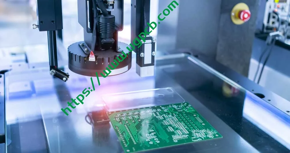
UGPCB의 표준 양면 스루홀 PCB 제조 공정:
1. 입고 자재 검사 → FR-4 동박적층판 두께 확인, 동박 품질, 그리고 시각적 결함.
2. 절단 → 대형 동박 적층판을 작업 패널 크기에 맞게 절단 (86.9 × 73.58 mm).
3. 교련 → 고정밀 CNC 드릴링 기계를 사용하여 Gerber 드릴 파일에 따라 모든 관통 구멍을 뚫습니다. (최소 직경 0.236 mm).
4. 도금 스루홀 (PTH) → 무전해 구리 증착을 통해 홀 벽에 얇은 구리 시드층 증착.
5. 패널 도금 → 구리를 전해 도금하여 홀벽과 표면 구리를 목표 두께로 형성 (1 온스).
6. 패턴 전송 → 라미네이트 드라이 필름, 폭로하다, 현상하여 회로 패턴 레지스트를 형성합니다..
7. 에칭 → 보호되지 않은 구리를 에칭하여 최종 회로 패턴 형성.
8. 스트리핑 → 회로 트레이스에서 레지스트 드라이 필름을 제거합니다..
9. 솔더 마스크 적용 → 녹색 솔더 마스크 잉크 도포, 폭로하다, 패드가 노출되도록 개발.
10. 표면 마감 → 무연 HASL.
11. 범례 인쇄 → 스크린 프린트 흰색 실크스크린 전설.
12. 라우팅 / V컷 → 최종 보드 아웃라인까지 CNC 라우팅.
13. 전기 테스트 → 개방/단락 무결성을 확인하기 위한 플라잉 프로브 또는 고정 장치 테스트.
14. 최종 품질 관리 (FQC) → 육안검사, 차원 샘플링, 그리고 배송을 위한 포장.
11. 응용 시나리오
UGPCB 양면 스루홀 FR-4 PCB 보드, 균형 잡힌 성능과 성숙한 프로세스로, 널리 사용됩니다:
11.1 가전제품
-
전원 어댑터 및 충전기
-
가전제품 제어반
-
스마트 홈 장치
11.2 산업 제어
-
PLC 프로그래밍 가능 논리 컨트롤러
-
산업용 전력 모듈
-
계측 및 미터
11.3 통신 장비
-
라우터 및 스위치
-
통신 모듈
-
신호 변환 장치
11.4 자동차 전자
-
온보드 충전기
-
차체 제어 모듈 (안전에 중요하지 않은)
-
인포테인먼트 시스템
11.5 의료 기기
-
환자 모니터 보조 보드
-
휴대용 의료 장비 (수업 2 해당되는)
12. 제품 장점 및 선택 가이드
12.1 UGPCB 양면 스루홀 PCB를 선택하는 이유?
-
IPC 준수 프로세스 제어 — 소재 선정부터 완제품까지, IPC-6012F를 완벽하게 준수, IPC-4101, 및 기타 국제 표준.
-
고정밀 제조 — 최소 구멍 직경 0.236 mm 및 최소 선폭 0.32 mm 매체를 만나다- 고밀도 설계 요구 사항에 맞춰.
-
환경 준수 — 무연 HASL 표면 마감은 RoHS를 준수합니다. 2.0 지시어.
-
입증된 신뢰성 — FR-4 기판은 일관된 성능으로 수십 년 동안 시장 검증을 거쳤습니다..
-
빠른 배송 — 표준 사양에 충분한 원자재가 구비되어 있습니다., 안정적인 리드타임 보장.
12.2 선택 참고
UGPCB 양면 스루홀 PCB는 프로젝트가 이러한 기준을 충족할 때 이상적인 선택입니다.:
-
적당한 회로 복잡성 2 레이어는 수용할 수 있습니다
-
아래의 작동 주파수 1 GHz (FR-4는 이 범위에서 탁월한 성능을 발휘합니다.)
-
120°C를 초과하지 않는 장기 작동 환경
-
높은 가치를 요구하는 비용에 민감한 애플리케이션
13세. 견적 요청
UGPCB는 전 세계 고객에게 고품질 PCB 제조 및 턴키 PCBA 서비스를 제공하기 위해 최선을 다하고 있습니다.. 표준 사양 양면 스루홀 PCB가 필요한지 아니면 맞춤형 요구 사항이 필요한지 여부 (특수 보드 두께, 구리 무게, 표면 마감, 임피던스 제어, 등.), UGPCB의 전문가 팀은 엔지니어링 설계부터 양산까지 전폭적인 지원을 제공합니다..
지금 견적을 받아보세요:
-
Gerber 파일 제출 + 사양 — 이내에 견적을 받으세요 24 시간
-
프로토타입부터 대량생산까지 지원
-
제조를 위한 자유로운 디자인 (DFM) 검토
UGPCB에 문의하세요:
📧 판매문의: [sales@ugpcb.com]
🌐 웹사이트: [www.ugpcb.com]
14세. 데이터 소스 선언
이 문서에 인용된 표준 및 데이터는 다음 권위 있는 기관에서 출처를 얻었습니다.:
-
IPC (전자산업을 연결하는 협회): IPC-6012F 경질 인쇄 기판의 자격 및 성능 사양 (구월 2023); IPC-4101 경질 및 다층 인쇄 기판용 기본 재료 사양; IPC-2221 인쇄 기판 설계에 대한 일반 표준; IPC-7351 표면 실장 설계 및 랜드 패턴 표준에 대한 일반 요구 사항
-
UL (보험업자 실험실): UL 94 기기 및 가전제품 부품용 플라스틱 재료의 난연성 시험에 대한 표준
-
아니요 (전국전기제조협회): FR-4 재료 등급 정의
-
산업 표준 기술 데이터: FR-4 유전 상수, 소산 인자, 및 기타 재료 특성 매개변수













