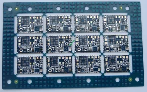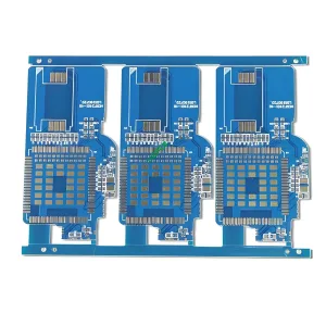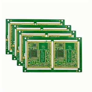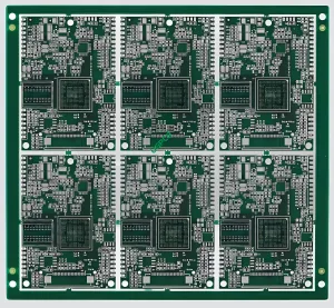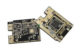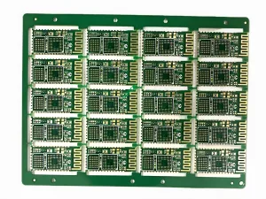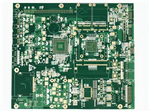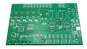
High-Performance 12-Layer ENIG + 골드 핑거 PCB 제품개요
그만큼 12-레이어 골드 핑거 PCB is a hallmark product in the high-end 인쇄 회로 기판 산업, engineered specifically for electronic equipment demanding extreme reliability, stable electrical connections, and frequent plugging/unplugging cycles. UGPCB employs advanced manufacturing processes and premium materials (FR-4 TG170), 결합 2중” 무전해 니켈 침지 금 (동의하다) surface finish with 30중” Hard Gold Finger Plating 기술. We deliver a comprehensive high-reliability PCB solution for applications ranging from industrial controls to advanced communication systems.
제품 정의
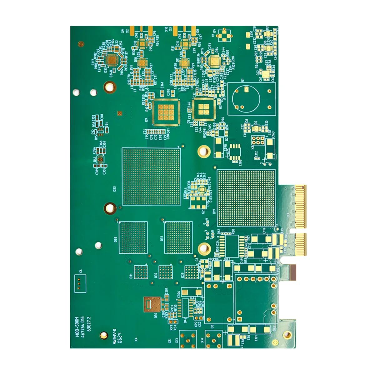
A Gold Finger PCB refers to a circuit board featuring a series of exposed, rectangular contact pads plated with thick gold (“fingers”) along one edge. These boards are designed for direct insertion into a matching connector slot, establishing a stable, pluggable connection for electrical signals and power between devices. 이 제품은 12-레이어 다층 PCB with a standard thickness of 1.60mm, offering an optimal balance between complex circuit integration and mechanical robustness.
중요한 설계 고려 사항
-
Gold Finger Area Design:
-
Chamfer (Bevel) Edge (Typically 20-45°): Facilitates smooth insertion into the connector—a critical aspect of 골드핑거 PCB 설계.
-
Lead-in (Trace Fanout): Connections from the gold fingers to internal traces must have smooth curves, avoiding right angles to prevent stress concentration and plating cracks.
-
Solder Mask Clearance (Solder Mask Define): The gold finger area requires precise solder mask opening to ensure a clean, exposed plating surface.
-
-
임피던스 제어 & 신호 무결성: 로서 12-layer precision PCB, strict impedance control (예를 들어, 50Ω 단일 종단, 100Ω 차동) for high-speed signal layers is essential. Stack-up design must be optimized via simulation to minimize crosstalk.
-
열의 & Reliability Management: High-Tg material, coupled with a well-designed via structure, ensures the 다층 PCB operates stably in elevated temperature environments. 홀을 통해 도금 (PTHS) should be avoided at the root of gold fingers to prevent fluid entrapment and structural weakness.
작동 방식 & 구조
This PCB facilitates complex circuit interconnections through its internal 12 전도성 층. The core functionality resides in the Hard Gold Plated Fingers. The durable 30-microinch gold plating provides excellent conductivity, 내산화성, 내마모성. When the board is inserted into a backplane or card-edge connector, the gold fingers make tight, low-resistance electrical contact with the connector’s spring contacts, transmitting signals and power. The board core uses FR-4 TG170, providing solid mechanical support and electrical insulation.
핵심 재료 & 명세서
-
기본 재료: FR-4 TG170. A high-performance epoxy glass laminate.
-
높은 유리 전이 온도 (Tg ≥ 170°C): Significantly enhances the PCB’s mechanical stability and heat resistance under high-temperature operating conditions, preventing delamination and Z-axis expansion.
-
우수한 전기적 특성: 저 유전 상수 (DK) 및 소산 인자 (Df), suitable for mid-to-high frequency applications.
-
High Mechanical Strength: Ensures the 1.6mm thick PCB board resists bending and warping in mating/unmating and high-vibration environments.
-
-
표면 마감:
-
Board Surface: 무전해 니켈 침지 금 (동의하다, 2중”): 아파트를 제공합니다, coplanar surface for reliable soldering of fine-pitch components and offers excellent oxidation resistance.
-
골드 핑거스: Selective Electroplated Hard Gold (30중”): High hardness, superior abrasion resistance, and extended mating cycle life, capable of withstanding 500+ insertion/withdrawal cycles with ease.
-
주요 특징 & 장점
-
Unmatched Reliability: FR-4 TG170 high-Tg material 그리고 12-layer precision lamination ensure long-term stability in harsh operating conditions.
-
Extended Mating Cycle Life: 30중” thick hard gold fingers far exceed standard plating thickness, offering exceptional wear resistance—the ideal choice for high-durability plug-in PCBs.
-
우수한 신호 무결성: The multilayer design provides uninterrupted reference planes for high-speed signals, and controlled impedance guarantees signal quality.
-
Robust Thermal & 기계적 성능: The 1.60mm standard thickness combined with high-Tg material delivers superior rigidity, 열 관리, and dimensional stability.
-
Comprehensive High-End Solution: 에서 다층 PCB 제작 에게 specialty surface finishing (동의하다 + Selective Gold), UGPCB provides full-process control, ensuring consistent, 고품질 결과.
제조 공정 흐름
Panelization → Inner Layer Imaging → Lamination (12-층) → Drilling → Desmear & Electroless Copper Deposition → Outer Layer Imaging → 패턴 도금 (for Hard Gold Fingers) → Etching → Solder Mask Application → ENIG 표면 마감 → Gold Finger Beveling → Electrical Test (비행 프로브 / Fixture) → 최종 자동 광학 검사 (AOI) → 포장.
기본 응용 프로그램 & 사용 사례
This product is the core component of high-end electronic devices requiring direct board-to-board plug connections 또는 integration into backplane systems.
-
산업 제어 시스템: PLC 모듈, industrial computer motherboards, 서보 드라이브, I/O interface cards.
-
통신 & Networking Equipment: Router/switch line cards, optical transceiver modules, baseband processing units.
-
의료 전자 장치: Data acquisition and processing boards for advanced medical imaging systems (예를 들어, CT 스캐너, ultrasound machines).
-
시험 & 측정 장비: Plug-in modules for high-end oscilloscopes, 스펙트럼 분석기, and Automated Test Equipment (먹었다).
-
항공우주 & 국방전자: Mission-critical avionics systems and radar signal processing modules where reliability is paramount.

과학적인 제품 분류
-
레이어 수에 의해: High-Layer-Count / 다층 회로 보드 (≥8 layers, 구체적으로 12 레이어).
-
By Special Feature/Process: 골드핑거 (Gold Edge Connector) PCB, Mixed Surface Finish PCB (동의하다 + Selective Hard Gold).
-
By Material Property: 높은 Tg (TG170) PCB, FR-4 Series PCB.
-
신청등급별: Industrial-Grade PCB, Telecom-Grade PCB, 고신뢰성 PCB.
Why Choose UGPCB’s 12-Layer Gold Finger PCB?
We understand that a reliable Gold Finger PCB is the foundation of your high-end equipment’s stable operation. 심층적인 전문 지식을 활용하여 다층 PCB 제조 그리고 specialty surface finish processes, UGPCB guarantees that every board delivered meets military-grade reliability standards with commercial-grade delivery efficiency. 우리는 단순한 제품이 아닌, but a customized PCB solution.
지금 기술 영업팀에 문의하세요 to discuss your project requirements, receive a detailed quote, and qualify for a free design-for-manufacturability (DFM) 검토 and sample program. Partner with UGPCB for your most demanding 12 레이어 회로 기판 애플리케이션.