

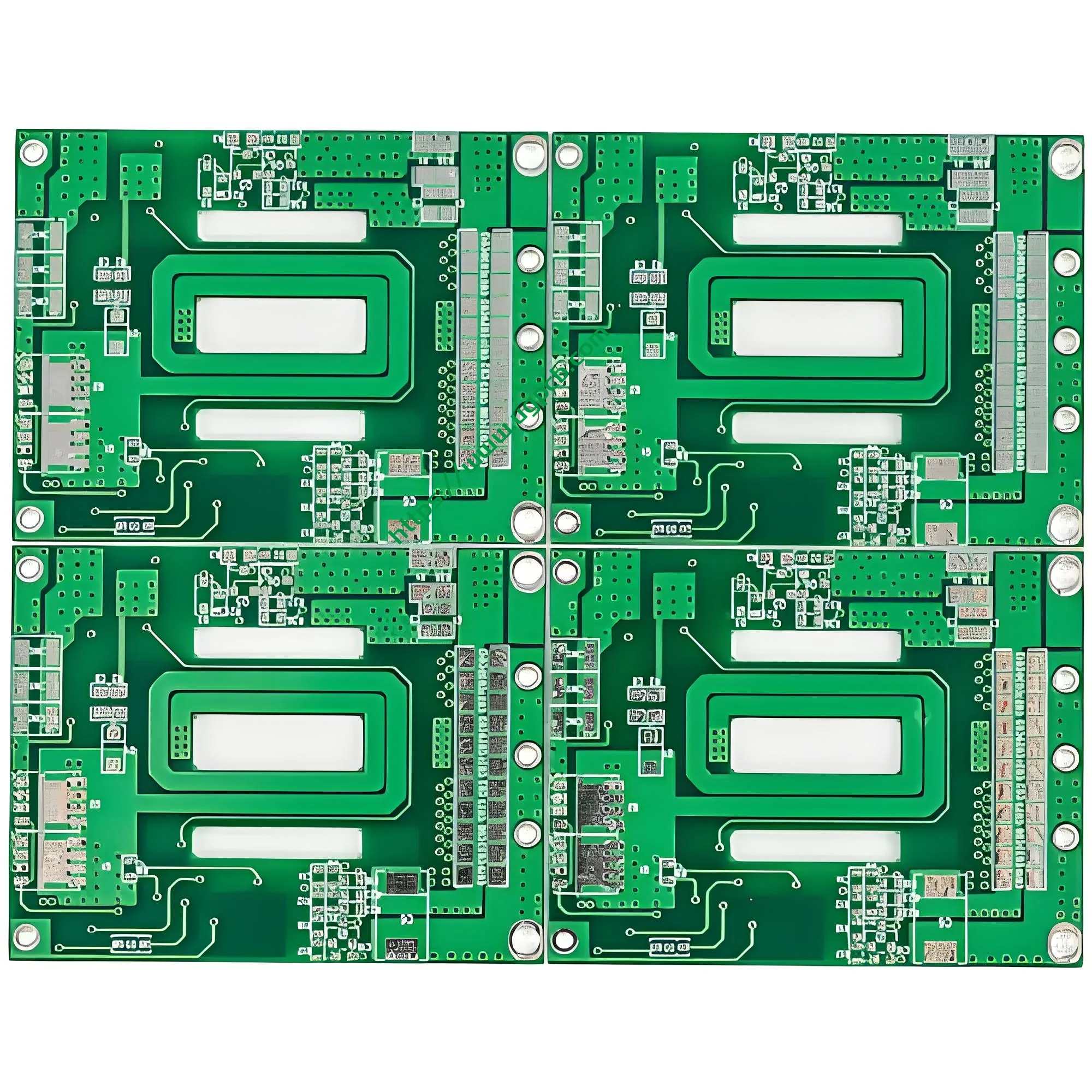
제품개요: What Is a Nickel-Palladium-Gold Double-Sided PCB?
A nickel-palladium-gold double-sided PCB (also known as an ENEPIG double-sided PCB) 는 인쇄 회로 기판 that features the Electroless Nickel Electroless Palladium Immersion Gold (에네픽) surface finish on both sides of the board. This advanced surface treatment builds upon the traditional double-sided PCB structure by adding a palladium layer between the nickel and gold deposits, creating a robust tri-layer composite finish that delivers superior solderability, wire bonding performance, and environmental stability.
UGPCB’s nickel-palladium-gold double-sided PCB uses Kingboard KB6160A FR-4 copper-clad laminate as the base material. 이사회에서 측정 49.6 × 32.8 mm 두께의 1.6 mm and a copper foil thickness of 1 온스 (약 35 μm). The solder mask is green with white silkscreen characters. 최소 조리개 0.27 mm and a minimum line width/spacing of 0.27 × 0.3 mm, this ENEPIG PCB delivers precision manufacturing combined with high-quality surface finishing.
The nickel-palladium-gold PCB is widely recognized as a “universal surface finish” in the electronics industry. It serves a broad range of applications, 통신 포함, 가전제품, 산업 제어, 보안 시스템, 자동차 전자, 전원 공급 장치, 스마트 홈 기기, 의료 장비, and military/aerospace systems.
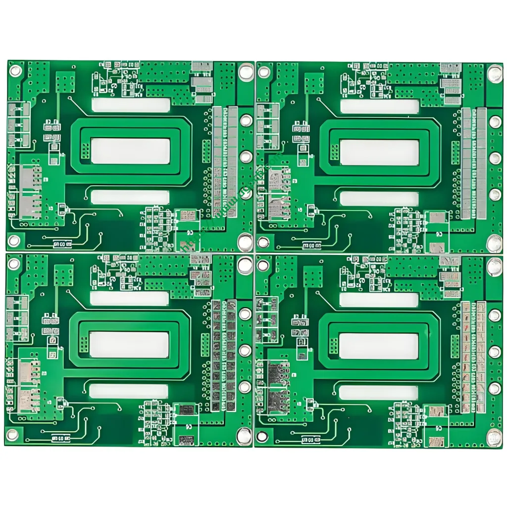
주요 기술 사양
| 매개 변수 | 사양 |
|---|---|
| 라미네이트 | Kingboard KB6160A FR-4 |
| 보드 두께 | 1.6 mm |
| 레이어 수 | 양면 |
| 보드 크기 | 49.6 × 32.8 mm |
| 최소 조리개 | 0.27 mm |
| 최소 선 너비/간격 | 0.27 × 0.3 mm |
| 동박 두께 | 1 온스 (≒35μm) |
| 표면 마감 | Nickel-Palladium-Gold (에네픽) |
| 솔더 마스크 / 전설 | 녹색 솔더 마스크 / 흰색 실크스크린 |
Laminate Details: KB6160A FR-4 Copper-Clad Laminate
KB6160A is a high-performance FR-4 copper-clad laminate manufactured by Kingboard Laminates Holdings Ltd. This material is specifically designed for standard double-sided printed wiring board (PWB) 조작. It complies with the IPC-4101/21 specification sheet. Key properties include:
- UV 차단 (UVB) 능력: Prevents light transmission during imaging, improving pattern transfer accuracy and yield
- 탁월한 치수 안정성: Ensures precision throughout the manufacturing process
- Superior heat resistance and mechanical properties: Meets high-reliability application requirements
- 유리전이온도 (Tg): 135℃ (DSC 방식)
- 열분해 온도 (Td): 305℃ (TGA method)
- z 축 Cte (A1/A2): 58 ppm/°C (< Tg) / 286 ppm/°C (> Tg)
- 유전 상수 (DK): 4.58
- 소산 인자 (Df): 0.022
- 부피 저항성: 1 × 10⁸ MΩ-cm
- 수분 흡수: 0.21%
- 가연성 등급: UL94V-0
(Data above are sourced from the Kingboard KB6160A Technical Data Sheet, with test methods per IPC-TM-650 series standards.)
The ENEPIG Surface Finish: A Detailed Explanation
What Is ENEPIG?
ENEPIG stands for Electroless Nickel Electroless Palladium Immersion Gold. It is an electroless chemical surface treatment that sequentially deposits three metal layers—nickel, 보장, and gold—onto the copper circuitry of a PCB.
The tri-layer structure of ENEPIG consists of:
- Bottom Layer – Electroless Nickel (~ 안에): Thickness of 3–5 μm. This layer acts as a diffusion barrier, preventing copper migration to the surface while providing mechanical support and a foundation for soldering.
- Middle Layer – Electroless Palladium (PD): Thickness of 0.05–0.1 μm. This critical barrier layer prevents interaction between nickel and gold, eliminating galvanic corrosion.
- Top Layer – Immersion Gold (au): Thickness of 0.03–0.05 μm. This thin layer provides excellent solderability and oxidation protection.
According to IPC-4556A (the latest 2025 개정), ENEPIG deposit thickness requirements are specified as follows:
- 니켈층: 3 μm ~ 6 μm (평균 ± 4σ로 측정됨)
- Palladium layer: 0.05 μm ~ 0.30 μm (평균 ± 4σ로 측정됨)
- 골드 레이어: Minimum 0.030 μm, 최고 0.07 μm (measured at below average − 4σ)
(Thickness specifications above are based on IPC-4556A, 무전해 니켈/무전해 팔라듐/침수 금 사양 (에네픽) Plating for Printed Boards.)
The ENEPIG Process Flow
UGPCB’s nickel-palladium-gold double-sided PCBs follow a standardized electroless plating process:
Degreasing → Micro-etching → Pre-dipping → Activation → Electroless Nickel Plating → Electroless Palladium Plating → Immersion Gold Plating → Drying
Each process step includes multiple rinsing stages to ensure plating quality and adhesion. The chemical reactions involved include both oxidation-reduction reactions and displacement reactions.
Core Advantages of Nickel-Palladium-Gold Double-Sided PCBs
1. Complete Elimination of the “Black Pad” Defect
The ENIG (무전해 니켈 침지 금) process has long been plagued by the “Black Pad” defect—a condition where gold attack on the nickel layer leads to brittle solder joints and premature failure. ENEPIG solves this problem by introducing a palladium barrier layer between nickel and gold, preventing direct contact and eliminating grain boundary corrosion. Industry data shows that ENEPIG reduces black pad occurrences by nearly 90% compared to ENIG. Under extreme temperature cycling conditions, ENEPIG demonstrates up to 30% higher reliability than ENIG.
2. Superior Wire Bonding Capability
ENEPIG surface finishes offer excellent bonding performance for both gold and aluminum wires. The palladium layer widens the process window for gold wire bonding, enabling reliable wire bonds even with thinner gold deposits. In many applications, ENEPIG supports wire bonding strengths exceeding 10 grams for both gold and aluminum wire bonds. This makes nickel-palladium-gold double-sided PCBs particularly suitable for semiconductor packaging and hybrid assembly applications requiring wire bonding.
3. Excellent Solderability and Multiple Reflow Tolerance
ENEPIG surface finishes provide excellent solderability with both leaded and lead-free solders (including SAC305 alloy). ENEPIG-finished PCBs can withstand up to 10 reflow cycles without significant degradation.
4. 유통기한 연장
Thanks to the protective palladium layer, ENEPIG surface finishes offer superior oxidation and corrosion resistance. This translates to a significantly longer shelf life compared to other surface finishes. According to IPC guidelines, ENEPIG surface finishes can achieve IPC Category 3 shelf life of at least twelve months.
5. Greater Design Flexibility
Unlike electrolytic nickel-gold processes, ENEPIG is an electroless process that requires no busbars or plating leads. This allows more boards to be processed simultaneously in the same plating bath, increasing overall throughput. 추가적으로, ENEPIG imposes no routing restrictions, providing greater flexibility for high-density circuit designs.
How Nickel-Palladium-Gold Double-Sided PCBs Work
The Synergistic Action of Three Plating Layers
The exceptional performance of nickel-palladium-gold double-sided PCBs stems from the precise synergy of the three plating layers:
① Nickel Layer (Ni-P Alloy) – The Foundation Barrier
The nickel layer serves as the foundation of the ENEPIG structure. Its primary function is to block copper atom diffusion to the surface, preventing the formation of brittle Cu-Sn intermetallic compounds (IMC) during soldering or high-temperature exposure. Nickel thickness is typically controlled between 3–6 μm, with phosphorus content strictly maintained at 7–9% to balance hardness and corrosion resistance.
② Palladium Layer (PD) – The Critical Barrier and Activation Layer
The palladium layer is the defining feature that distinguishes ENEPIG from ENIG. It acts as a “partition wall,” preventing migration and grain boundary corrosion between nickel and gold. The palladium layer must be thick enough to block nickel diffusion to the gold surface and prevent excessive corrosion of the electroless nickel deposit.
③ Gold Layer (au) – Protection and Solderability
The thin outer gold layer protects the nickel from oxidation while providing low contact resistance and excellent solderability. Because the palladium layer provides isolation, the gold layer in ENEPIG can be made thinner (0.03-0.05μm) without compromising reliability, which helps reduce material costs to some extent.
Classification of Nickel-Palladium-Gold Double-Sided PCBs
UGPCB’s nickel-palladium-gold double-sided PCB can be scientifically classified across multiple dimensions:
By Number of Layers
- 양면 PCB: Conductive circuits are distributed on both sides of the substrate, with electrical connections established through plated through-holes (PTHS).
기본 재료에 의해
- FR-4 에폭시 유리 직물 라미네이트: Using Kingboard KB6160A, compliant with IPC-4101/21.
표면 마감별
- 에네픽 (전기 니켈 전기 팔라듐 침지 금) : Tri-layer composite plating structure.
애플리케이션 도메인별
- High-Reliability General-Purpose PCB: Suitable for telecommunications, 자동차 전자, 의료기기, 항공우주, 산업 제어, 그리고 더.
By Manufacturing Precision
- 정밀 PCB: Minimum aperture of 0.27 mm, minimum line width/spacing of 0.27 × 0.3 mm.
제조 공정 흐름
UGPCB’s nickel-palladium-gold double-sided PCB production follows a comprehensive manufacturing workflow:
단계 1: 기판 준비
- 재료 절단: KB6160A copper-clad laminate is cut to the required dimensions.
- 교련: Mechanical drilling with a minimum aperture of 0.27 mm.
- 무전해 구리 증착 & 패널 도금: Through-hole metallization.
단계 2: 회로 형성
- 패턴 전송: Dry film lamination → Exposure → Development.
- 회로 에칭: Removal of excess copper to form the circuit pattern.
- AOI (자동 광학 검사) : Ensuring circuit accuracy.
단계 3: 솔더 마스크 및 범례
- 솔더 마스크 인쇄: Green ink application to protect circuits and prevent solder bridging.
- 범례 인쇄: White silkscreen characters.
단계 4: 표면 마감 (에네픽)
- 탈지: Removal of surface contaminants.
- 마이크로 에칭: Light etching of copper surface to enhance adhesion.
- Pre-Dipping: Pretreatment before activation.
- 활성화: Deposition of catalytic palladium seed layer on copper.
- Electroless Nickel Plating: Deposition of nickel layer (3–5 μm).
- Electroless Palladium Plating: Deposition of palladium layer (0.05-0.1μm).
- Immersion Gold Plating: Deposition of gold layer (0.03-0.05μm).
- 건조: Completion of surface finish.
단계 5: 최종검사
- 전기 테스트: Ensuring electrical continuity and isolation.
- 육안검사: Checking surface quality.
- 포장 & 해운.
일반적인 응용 프로그램
UGPCB’s nickel-palladium-gold double-sided PCBs are widely used across numerous industries:
통신 장비
- 기지국, 라우터, 스위치
- High-frequency communication modules, RF devices
자동차 전자
- 엔진 제어 장치 (씌우다)
- 차량 내 인포테인먼트 시스템
- ADAS (고급 운전자 지원 시스템)
- BMS (배터리 관리 시스템) for new energy vehicles

의료 기기
- Medical implantable devices
- Diagnostic instruments, 환자 모니터링 장비
항공우주 & 방어
- Spacecraft and satellite electronics
- Aviation control systems
산업 제어 & 보안
- PLC (Programmable Logic Controllers)
- Industrial motor drives
- Security and surveillance equipment
가전제품 & 스마트 홈
- Smartphone motherboards
- Smart home control modules
- 웨어러블 기기
군대 & 전력전자
- Military electronic systems
- 전원 모듈, power converters
Why Choose UGPCB for Nickel-Palladium-Gold Double-Sided PCBs?
✅ IPC Standards Compliance
UGPCB’s nickel-palladium-gold double-sided PCBs are manufactured in strict accordance with IPC-4556A. The KB6160A laminate complies with IPC-4101/21, ensuring full standardization from base material to surface finish.
✅ 정밀 제조 역량
최소 조리개 0.27 mm 및 최소 선 너비/간격 0.27 × 0.3 mm, UGPCB meets the demands of high-density interconnect (HDI) and fine-pitch component assembly.
✅ High-Reliability Assurance
ENEPIG surface finish reduces black pad defects by nearly 90% and delivers up to 30% higher reliability than ENIG under extreme temperature fluctuations. Products withstand multiple reflow cycles and meet J-STD-003 범주 3 durability requirements.
✅ Professional Technical Support
The UGPCB team provides full-process technical support, from Gerber file review and BOM optimization to PCBA assembly.
Inquiries & Ordering
Ready to turn your design into a high-quality nickel-palladium-gold double-sided PCB?
📧 이메일: sales@ugpcb.com
📞 전화: +86-135 4412 8719
🌐 웹사이트: www.ugpcb.com
📋 Ordering Process:
- Gerber 파일 제출, BOM, and design documentation.
- UGPCB’s engineering team performs DFM (제조 가능성을위한 설계) 검토.
- Order confirmation and delivery schedule.
- Manufacturing and quality control.
- Shipping and logistics tracking.
당신이 필요 여부 PCB 프로토 타이핑 또는 대량 생산, UGPCB is committed to delivering high-quality nickel-palladium-gold double-sided PCBs and professional technical services.
데이터 소스 선언
The technical data and standard specifications cited in this document are sourced from the following authoritative organizations:
- IPC-4556A: 무전해 니켈/무전해 팔라듐/침수 금 사양 (에네픽) 인쇄 기판용 도금 (2025 개정)
- IPC-4101/21: 경질 및 다층 인쇄 기판용 기본 재료 사양 – the specification sheet applicable to KB6160A
- Kingboard KB6160A Technical Data Sheet (Kingboard Laminates Holdings Ltd.)
- IPC-TM-650: 테스트 방법 매뉴얼 – the standard test methods used for material property measurements
- J-성병-003: 인쇄 기판의 납땜성 테스트 – the solderability testing standard
- UL94: 기기 및 가전제품 부품용 플라스틱 재료의 난연성 시험에 대한 표준 – flammability rating standard
All data cited above are sourced from the official standards and technical documents listed, ensuring accuracy and authority.













