

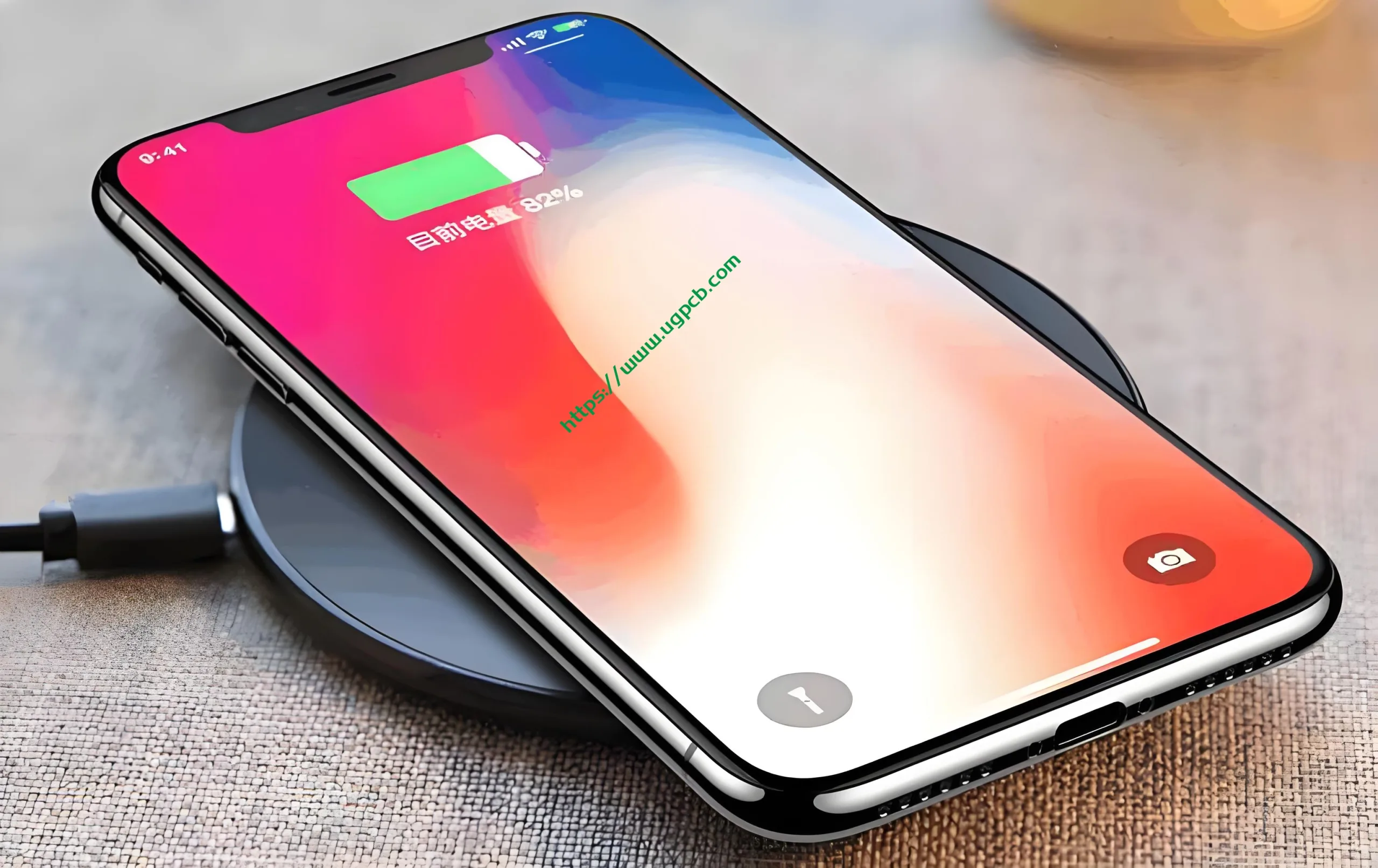
Introduction to Wireless Charging PCB
A Wireless Charging PCB, also known as an inductive charging 회로 기판, is a specialized printed circuit board designed for wireless power transfer. It enables devices such as smartphones, 정제, and other electronic gadgets to be charged without the need for physical connectors.
작동 원리
Wireless charging technology operates on the principle of electromagnetic induction. The transmitter coil generates an alternating electromagnetic field that induces a current in the receiver coil, thus transferring energy from the charger to the device.
응용
Wireless Charging PCBs are widely used in consumer electronics for charging devices like mobile phones, 스마트워치, 이어폰, and even electric toothbrushes. They offer convenience, ease of use, and reduced wear and tear on charging ports.
Types of Wireless Charging PCBs
There are two main types of wireless charging technologies:
- Qi Standard: The most common and widely adopted wireless charging standard.
- PMA (Power Matters Alliance): Another popular standard, often found in older devices.
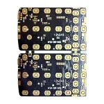
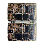
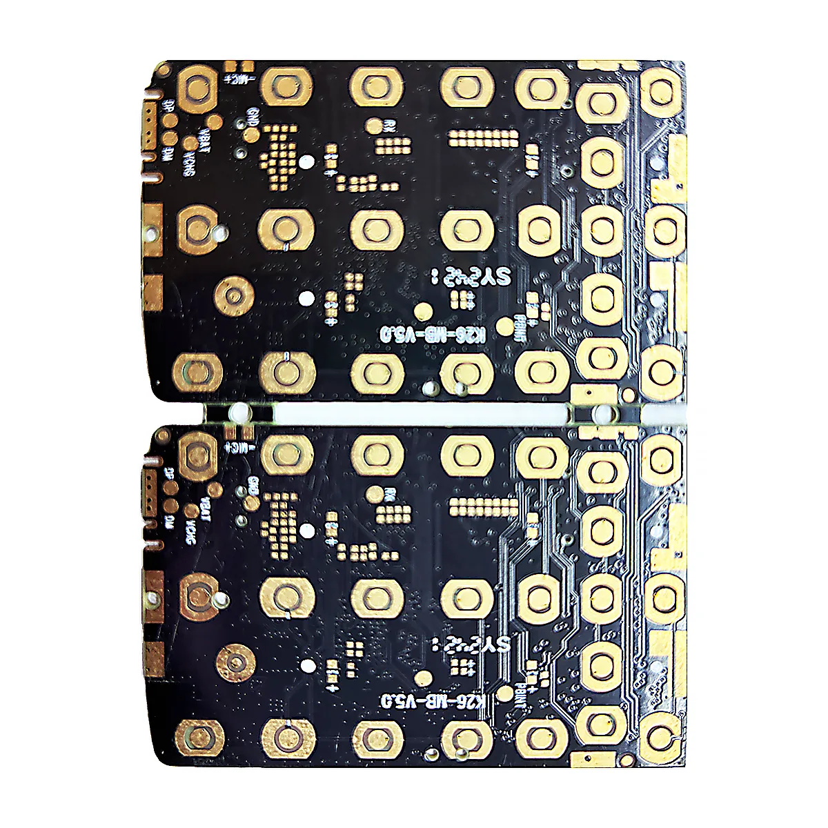
재료 및 건축
- 재료: S1000-2, 고품질 에폭시 소재.
- 레이어: 6 레이어, 견고성과 더 나은 신호 무결성 제공.
- 색상: 녹색 또는 흰색으로 제공됩니다..
- 완성된 두께: 1.2mm, 슬림하면서도 내구성을 확보한.
- 구리 두께: 2온스, 좋은 전도성을 제공하는.
- 표면 처리: Immersion gold with a thickness of at least 2U”, 내식성 및 납땜성 향상.
- 구멍의 구리 두께: 35하나, ensuring strong connections.
- 최소 조리개: 0.4mm, allowing for fine detail work.
성능 특성
Wireless Charging PCBs are designed to efficiently transfer power with minimal loss. They support fast charging capabilities and are built to withstand repeated usage over time. 침수 금 마감으로 오래 지속되는 성능과 신뢰성을 보장합니다..
구조적 특징
The structure of a Wireless Charging PCB includes multiple layers of copper traces sandwiched between layers of substrate material. 이 다층 설계는 열 방출을 관리하고 전기 성능을 향상시키는 데 도움이 됩니다.. 그만큼 PCB is coated with a protective layer to prevent damage and ensure longevity.
생산 과정
The production of a Wireless Charging PCB involves several steps:
- 설계: 전문 소프트웨어를 사용하여 회로 레이아웃 생성.
- 에칭: 원하는 패턴을 형성하기 위해 과도한 구리를 제거합니다..
- 라미네이션: 여러 레이어를 함께 결합.
- 도금: 연결성 향상을 위해 얇은 금속층 추가.
- 점검: PCB가 품질 표준을 충족하는지 확인.
- 집회: PCB에 부품 장착.
- 테스트: 기능 및 성능 검증.

사용 사례
Wireless Charging PCBs are used in various applications including:
- 가전제품: 휴대 전화, 정제, 스마트워치.
- 자동차: In-car charging systems for smartphones.
- 의료 기기: 휴대용 의료 장비.
- 웨어러블: Fitness trackers, smart rings.
결론적으로, Wireless Charging PCBs represent a significant advancement in charging technology, offering convenience, 능률, 그리고 내구성. 다양한 산업 전반에 걸쳐 광범위하게 채택되어 현대 전자 장치의 다양성과 중요성을 강조합니다..


