

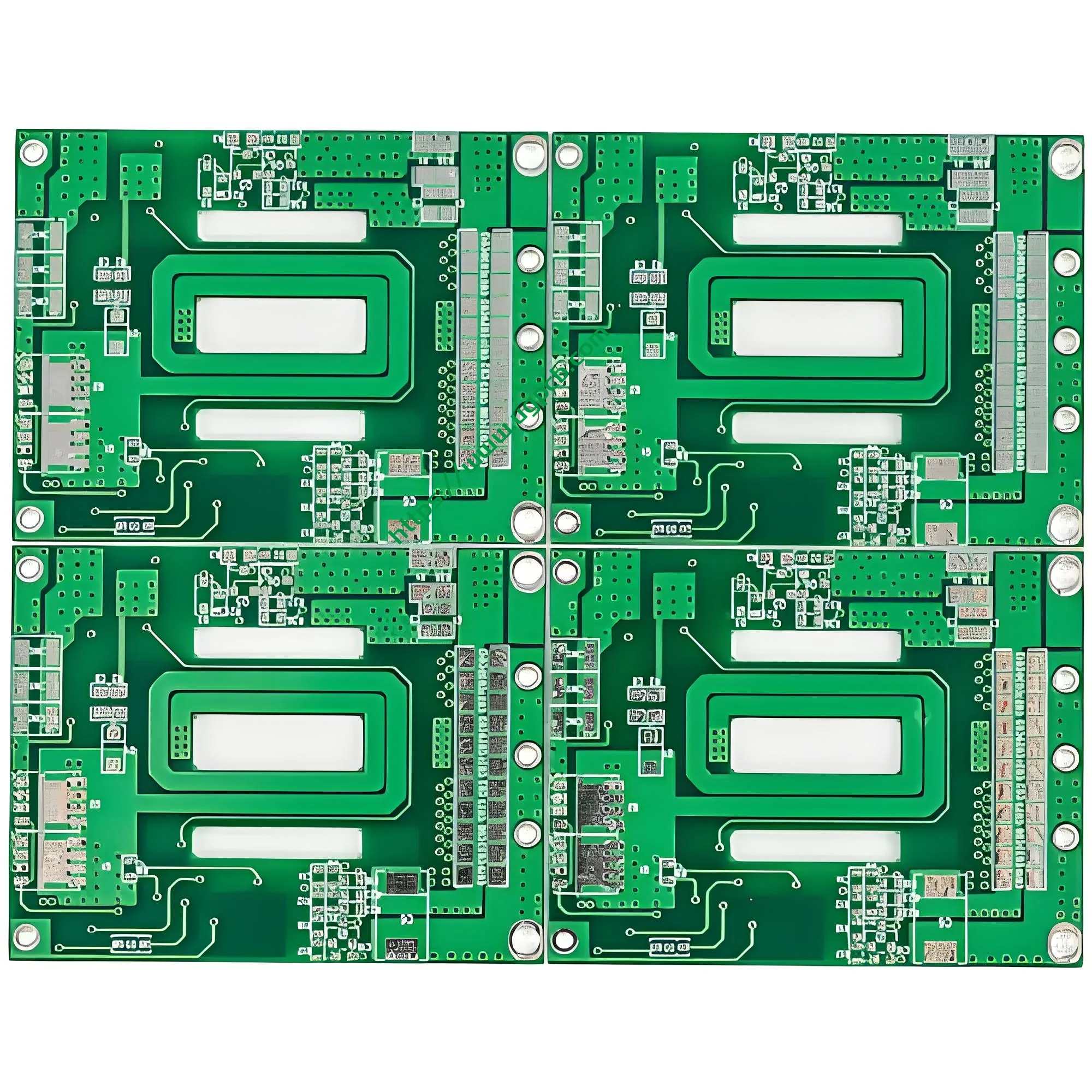
Visão geral do produto: O que é uma PCB dupla face de níquel-paládio-ouro?
Uma PCB dupla face de níquel-paládio-ouro (também conhecido como PCB de dupla face ENEPIG) é um placa de circuito impresso que apresenta o Ouro de Imersão Electroless Níquel Electroless Palladium (Enepic) acabamento superficial em ambos os lados da placa. Este tratamento de superfície avançado baseia-se na estrutura tradicional de PCB de dupla face, adicionando uma camada de paládio entre os depósitos de níquel e ouro, criando um acabamento composto de três camadas robusto que oferece soldabilidade superior, desempenho de ligação de fio, e estabilidade ambiental.
A PCB dupla face de níquel-paládio-ouro da UGPCB usa laminado revestido de cobre Kingboard KB6160A FR-4 como material de base. A diretoria mede 49.6 × 32.8 mm com espessura de 1.6 mm e uma espessura de folha de cobre de 1 onças (aproximadamente 35 μm). A máscara de solda é verde com caracteres em serigrafia branca. Com uma abertura mínima de 0.27 mm e uma largura/espaçamento mínimo de linha de 0.27 × 0.3 milímetros, este ENEPIG PCB oferece fabricação de precisão combinada com acabamento superficial de alta qualidade.
O PCB de níquel-paládio-ouro é amplamente reconhecido como um “acabamento de superfície universal” na indústria eletrônica. Serve para uma ampla gama de aplicações, incluindo telecomunicações, eletrônica de consumo, controle industrial, sistemas de segurança, eletrônica automotiva, Fontes de alimentação, dispositivos domésticos inteligentes, Equipamento médico, e sistemas militares/aeroespaciais.
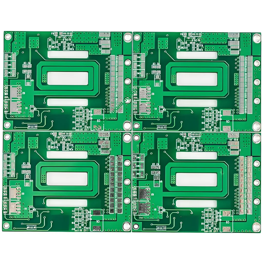
Principais especificações técnicas
| Parâmetro | Especificação |
|---|---|
| Laminado | Kingboard KB6160A FR-4 |
| Espessura da placa | 1.6 milímetros |
| Número de camadas | Frente e verso |
| Tamanho da placa | 49.6 × 32.8 milímetros |
| Abertura Mínima | 0.27 milímetros |
| Largura/espaçamento mínimo da linha | 0.27 × 0.3 milímetros |
| Espessura da folha de cobre | 1 onças (≈35 μm) |
| Acabamento superficial | Níquel-Paládio-Ouro (Enepic) |
| Máscara de solda / Lenda | Máscara de solda verde / Serigrafia branca |
Detalhes laminados: Laminado revestido de cobre KB6160A FR-4
KB6160A é um laminado revestido de cobre FR-4 de alto desempenho fabricado pela Kingboard Laminates Holdings Ltd. Este material foi projetado especificamente para placas de fiação impressas frente e verso padrão (PWB) fabricação. Está em conformidade com a folha de especificações IPC-4101/21. As principais propriedades incluem:
- Bloqueio UV (UVB) capacidade: Impede a transmissão de luz durante a geração de imagens, melhorando a precisão e o rendimento da transferência de padrões
- Excelente estabilidade dimensional: Garante precisão em todo o processo de fabricação
- Resistência ao calor e propriedades mecânicas superiores: Atende aos requisitos de aplicações de alta confiabilidade
- Temperatura de transição vítrea (Tg): 135°C (Método DSC)
- Temperatura de decomposição térmica (Td): 305°C (Método TGA)
- Zis Z CTE (a1/a2): 58 ppm/°C (< Tg) / 286 ppm/°C (> Tg)
- Constante dielétrica (Dk): 4.58
- Fator de dissipação (Df): 0.022
- Resistividade de volume: 1 × 10⁸ MΩ-cm
- Absorção de umidade: 0.21%
- Classificação inflamabilidade: UL94V-0
(Os dados acima são provenientes da Ficha Técnica Kingboard KB6160A, com métodos de teste de acordo com os padrões da série IPC-TM-650.)
O Acabamento de Superfície ENEPIG: Uma explicação detalhada
O que é ENEPIG?
ENEPIG significa Electroless Nickel Electroless Palladium Immersion Gold. É um tratamento de superfície químico sem eletrólito que deposita sequencialmente três camadas de metal – níquel, paládio, e ouro - no circuito de cobre de um PCB.
A estrutura de três camadas do ENEPIG consiste em:
- Camada Inferior – Níquel Electroless (Em): Espessura de 3–5 μm. Esta camada atua como uma barreira de difusão, evitando a migração de cobre para a superfície, ao mesmo tempo que fornece suporte mecânico e uma base para soldagem.
- Camada intermediária – paládio eletrolítico (PD): Espessura de 0,05–0,1 μm. Esta camada de barreira crítica evita a interação entre o níquel e o ouro, eliminando a corrosão galvânica.
- Camada Superior – Ouro de Imersão (Au): Espessura de 0,03–0,05 μm. Esta camada fina proporciona excelente soldabilidade e proteção contra oxidação.
De acordo com IPC-4556A (o mais recente 2025 revisão), Os requisitos de espessura do depósito ENEPIG são especificados como segue:
- Camada de níquel: 3 μm para 6 μm (medido em média ± 4σ)
- Camada de paládio: 0.05 μm para 0.30 μm (medido em média ± 4σ)
- Camada de ouro: Mínimo 0.030 μm, máximo 0.07 μm (medido abaixo da média - 4σ)
(As especificações de espessura acima são baseadas em IPC-4556A, Especificação para níquel eletrolítico/paládio eletrolítico/ouro de imersão (Enepic) Chapeamento para placas impressas.)
O Fluxo do Processo ENEPIG
Os PCBs dupla face de níquel-paládio-ouro da UGPCB seguem um processo padronizado de galvanização sem eletrodo:
Desengorduramento → Micro-gravação → Pré-imersão → Ativação → Niquelagem eletrolítica → Revestimento de paládio eletrolítico → Revestimento de ouro por imersão → Secagem
Cada etapa do processo inclui vários estágios de enxágue para garantir a qualidade e adesão do revestimento. As reações químicas envolvidas incluem reações de oxidação-redução e reações de deslocamento..
Principais vantagens dos PCBs dupla face de níquel-paládio-ouro
1. Eliminação completa do defeito “Black Pad”
O ENIG (Ouro de imersão em níquel eletrolítico) O processo há muito tempo é afetado pelo defeito “Black Pad” – uma condição em que o ataque do ouro na camada de níquel leva a juntas de solda quebradiças e falhas prematuras. ENEPIG resolve este problema introduzindo uma camada de barreira de paládio entre o níquel e o ouro, evitando o contato direto e eliminando a corrosão dos limites dos grãos. Dados da indústria mostram que o ENEPIG reduz a ocorrência de blocos pretos em quase 90% em comparação com ENIG. Sob condições extremas de ciclagem de temperatura, ENEPIG demonstra até 30% maior confiabilidade do que ENIG.
2. Capacidade superior de ligação de fios
Os acabamentos superficiais ENEPIG oferecem excelente desempenho de colagem para fios de ouro e alumínio. A camada de paládio amplia a janela do processo para colagem de fios de ouro, permitindo ligações eletrônicas confiáveis mesmo com depósitos de ouro mais finos. Em muitas aplicações, ENEPIG suporta forças de ligação de fios superiores 10 gramas para títulos de fios de ouro e alumínio. Isso torna os PCBs de dupla face de níquel-paládio-ouro particularmente adequados para embalagens de semicondutores e aplicações de montagem híbrida que exigem ligação de fios.
3. Excelente soldabilidade e tolerância a múltiplos refluxos
Os acabamentos de superfície ENEPIG proporcionam excelente soldabilidade com soldas com e sem chumbo (incluindo liga SAC305). PCBs com acabamento ENEPIG podem suportar até 10 ciclos de refluxo sem degradação significativa.
4. Vida útil estendida
Graças à camada protetora de paládio, Os acabamentos de superfície ENEPIG oferecem resistência superior à oxidação e à corrosão. Isto se traduz em uma vida útil significativamente mais longa em comparação com outros acabamentos de superfície. De acordo com as diretrizes do IPC, Os acabamentos de superfície ENEPIG podem atingir a categoria IPC 3 prazo de validade de pelo menos doze meses.
5. Maior flexibilidade de design
Ao contrário dos processos eletrolíticos de níquel-ouro, ENEPIG é um processo sem eletricidade que não requer barramentos ou cabos de chapeamento. Isto permite que mais placas sejam processadas simultaneamente no mesmo banho de galvanização, aumentando o rendimento geral. Adicionalmente, ENEPIG não impõe restrições de roteamento, proporcionando maior flexibilidade para projetos de circuitos de alta densidade.
Como funcionam os PCBs dupla face de níquel-paládio-ouro
A ação sinérgica de três camadas de revestimento
O desempenho excepcional dos PCBs de dupla face de níquel-paládio-ouro decorre da sinergia precisa das três camadas de revestimento:
① Camada de Níquel (Liga Ni-P) – A Barreira da Fundação
A camada de níquel serve de base da estrutura ENEPIG. Sua principal função é bloquear a difusão do átomo de cobre para a superfície, evitando a formação de compostos intermetálicos Cu-Sn frágeis (CMI) durante soldagem ou exposição a altas temperaturas. A espessura do níquel é normalmente controlada entre 3–6 μm, com teor de fósforo estritamente mantido em 7–9% para equilibrar dureza e resistência à corrosão.
② Camada de paládio (PD) – A barreira crítica e a camada de ativação
A camada de paládio é a característica definidora que distingue ENEPIG de ENIG. Funciona como uma “parede divisória,”prevenindo a migração e a corrosão dos limites de grão entre o níquel e o ouro. A camada de paládio deve ser espessa o suficiente para bloquear a difusão do níquel para a superfície do ouro e evitar a corrosão excessiva do depósito de níquel sem eletrólito..
③ Camada Dourada (Au) – Proteção e soldabilidade
A fina camada externa de ouro protege o níquel da oxidação, proporcionando baixa resistência de contato e excelente soldabilidade. Porque a camada de paládio fornece isolamento, a camada de ouro no ENEPIG pode ser mais fina (0.03–0,05 μm) sem comprometer a confiabilidade, o que ajuda a reduzir os custos de material até certo ponto.
Classificação de PCBs dupla face de níquel-paládio-ouro
O PCB dupla face de níquel-paládio-ouro da UGPCB pode ser classificado cientificamente em múltiplas dimensões:
Por número de camadas
- PCB de dupla face: Os circuitos condutores são distribuídos em ambos os lados do substrato, com conexões elétricas estabelecidas através de furos banhados (PThs).
Por material base
- Laminado de tecido de vidro epóxi FR-4: Usando KingBoard KB6160A, compatível com IPC-4101/21.
Por acabamento superficial
- Enepic (Gold de imersão com eletrólito com níquel de níquel) : Estrutura de revestimento composto de três camadas.
Por domínio de aplicativo
- PCB de uso geral de alta confiabilidade: Adequado para telecomunicações, eletrônica automotiva, dispositivos médicos, aeroespacial, controle industrial, e mais.
Por Fabricação de Precisão
- PCB de precisão: Abertura mínima de 0.27 milímetros, largura/espaçamento mínimo de linha de 0.27 × 0.3 milímetros.
Fluxo do Processo de Fabricação
A produção de PCB dupla face de níquel-paládio-ouro da UGPCB segue um fluxo de trabalho de fabricação abrangente:
Estágio 1: Preparação de substrato
- Corte de materiais: O laminado revestido de cobre KB6160A é cortado nas dimensões exigidas.
- Perfuração: Perfuração mecânica com abertura mínima de 0.27 milímetros.
- Deposição de cobre eletrolítico & Chapeamento de painel: Metalização através do furo.
Estágio 2: Formação de Circuito
- Transferência de padrão: Laminação de filme seco → Exposição → Revelação.
- Gravura de Circuito: Remoção do excesso de cobre para formar o padrão do circuito.
- AOI (Inspeção óptica automatizada) : Garantindo a precisão do circuito.
Estágio 3: Máscara de solda e legenda
- Impressão de máscara de solda: Aplicação de tinta verde para proteger circuitos e evitar pontes de solda.
- Impressão de legenda: Personagens em serigrafia branca.
Estágio 4: Acabamento superficial (Enepic)
- Desengordurante: Remoção de contaminantes superficiais.
- Micro-Gravação: Gravura leve da superfície de cobre para melhorar a adesão.
- Pré-mergulho: Pré-tratamento antes da ativação.
- Ativação: Deposição de camada catalítica de sementes de paládio em cobre.
- Niquelagem eletrolítica: Deposição de camada de níquel (3–5 μm).
- Chapeamento de paládio eletrolítico: Deposição de camada de paládio (0.05–0,1 μm).
- Chapeamento de ouro de imersão: Deposição de camada de ouro (0.03–0,05 μm).
- Secagem: Conclusão do acabamento superficial.
Estágio 5: Inspeção Final
- Teste elétrico: Garantindo continuidade elétrica e isolamento.
- Inspeção Visual: Verificando a qualidade da superfície.
- Embalagem & Envio.
Aplicações Típicas
Os PCBs dupla face de níquel-paládio-ouro da UGPCB são amplamente utilizados em vários setores:
Equipamentos de Telecomunicações
- Estações base, roteadores, interruptores
- Módulos de comunicação de alta frequência, Dispositivos RF
Eletrônica Automotiva
- Unidades de controle do motor (ECUs)
- Sistemas de infoentretenimento no veículo
- ADAS (Sistemas avançados de assistência ao motorista)
- Bms (Sistemas de gerenciamento de bateria) para novos veículos energéticos

Dispositivos médicos
- Dispositivos médicos implantáveis
- Instrumentos de diagnóstico, equipamento de monitoramento de pacientes
Aeroespacial & Defesa
- Eletrônica de naves espaciais e satélites
- Sistemas de controle de aviação
Controle industrial & Segurança
- Plc (Controladores lógicos programáveis)
- Acionamentos de motores industriais
- Equipamentos de segurança e vigilância
Eletrônicos de consumo & Casa inteligente
- Placas-mãe para smartphones
- Módulos de controle residencial inteligente
- Dispositivos vestíveis
Militares & Eletrônica de Potência
- Sistemas eletrônicos militares
- Módulos de potência, conversores de energia
Por que escolher UGPCB para PCBs dupla face de níquel-paládio-ouro?
✅ Conformidade com os padrões IPC
Os PCBs dupla face de níquel-paládio-ouro da UGPCB são fabricados em estrita conformidade com IPC-4556A. O laminado KB6160A está em conformidade com IPC-4101/21, garantindo total padronização desde o material base até o acabamento superficial.
✅ Capacidades de fabricação de precisão
Com uma abertura mínima de 0.27 mm e largura/espaçamento mínimo de linha de 0.27 × 0.3 milímetros, UGPCB atende às demandas de interconexão de alta densidade (IDH) e montagem de componentes de passo fino.
✅ Garantia de alta confiabilidade
O acabamento superficial ENEPIG reduz os defeitos da almofada preta em quase 90% e entrega até 30% maior confiabilidade do que ENIG sob flutuações extremas de temperatura. Os produtos suportam vários ciclos de refluxo e atendem ao J-STD-003 Categoria 3 requisitos de durabilidade.
✅ Suporte Técnico Profissional
A equipe UGPCB fornece suporte técnico completo ao processo, desde revisão de arquivo Gerber e otimização de BOM até montagem de PCBA.
Consultas & Pedido
Pronto para transformar seu design em uma PCB dupla face de níquel-paládio-ouro de alta qualidade?
📧 E-mail: vendas@ugpcb.com
📞 Telefone: +86-135 4412 8719
🌐 Site: www.ugpcb.com
📋 Processo de pedido:
- Envie arquivos Gerber, Bom, e documentação de projeto.
- A equipe de engenharia da UGPCB realiza DFM (Design para fabricação) análise.
- Confirmação do pedido e cronograma de entrega.
- Fabricação e controle de qualidade.
- Acompanhamento de remessa e logística.
Se você precisa Prototipagem de PCB ou produção em volume, A UGPCB está comprometida em fornecer PCBs dupla face de níquel-paládio-ouro de alta qualidade e serviços técnicos profissionais.
Declaração de fonte de dados
Os dados técnicos e especificações padrão citados neste documento são provenientes das seguintes organizações autorizadas:
- IPC-4556A: Especificação para níquel eletrolítico/paládio eletrolítico/ouro de imersão (Enepic) Chapeamento para placas impressas (2025 revisão)
- IPC-4101/21: Especificação de materiais básicos para placas impressas rígidas e multicamadas – a folha de especificações aplicável ao KB6160A
- Ficha Técnica Kingboard KB6160A (Kingboard Laminados Holdings Ltd.)
- IPC-TM-650: Manual de Métodos de Teste – os métodos de teste padrão usados para medições de propriedades de materiais
- J-STD-003: Testes de soldabilidade para placas impressas – o padrão de teste de soldabilidade
- UL94: Norma para testes de inflamabilidade de materiais plásticos para peças em dispositivos e eletrodomésticos – padrão de classificação de inflamabilidade
Todos os dados citados acima são provenientes dos padrões oficiais e documentos técnicos listados, garantindo precisão e autoridade.













