UGPCB: World-Leading PCB Manufacturer – High-Precision Circuit Board Production, Quick-Turn Prototyping & Stencil Solutions
Core Value of PCB Manufacturing & Industry Challenges
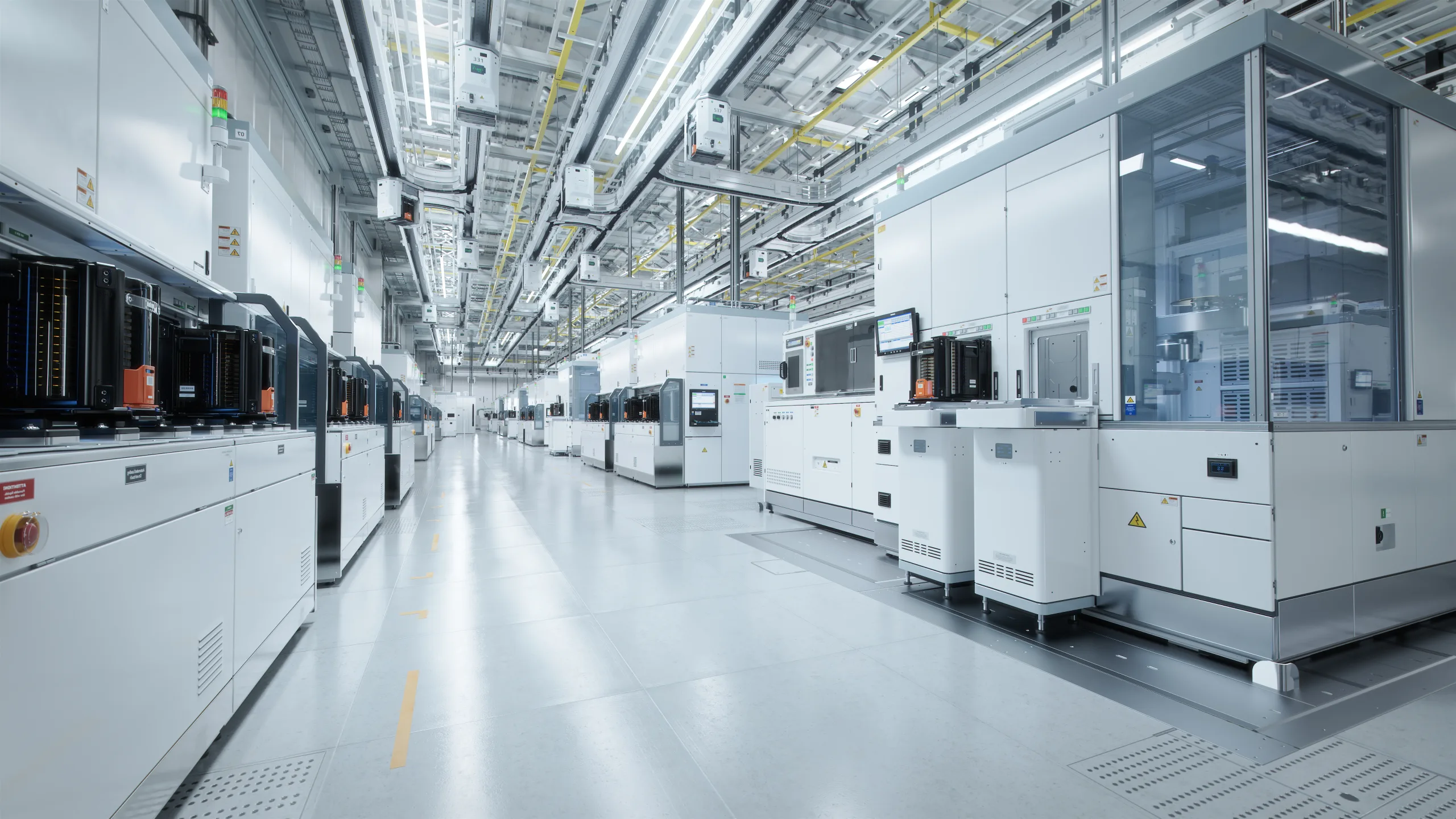
As the “skeleton” of electronic devices, PCB -uri directly impact product performance and cost. Industry statistics indicate PCBs account for 12%-18% of total electronic product costs, and quality defects can increase post-production repair costs by 300% (IPC standards data). UGPCB leverages its 28,000 m² modern facility and 1300-person professional team (35% technical experts) to specialize in solving high-end manufacturing challenges like high-frequency microwave PCBs, Panouri HDI, şi substraturi IC.
Three Core Capabilities: UGPCB’s Manufacturing Advantages
1. Scalable PCB Production Capacity
-
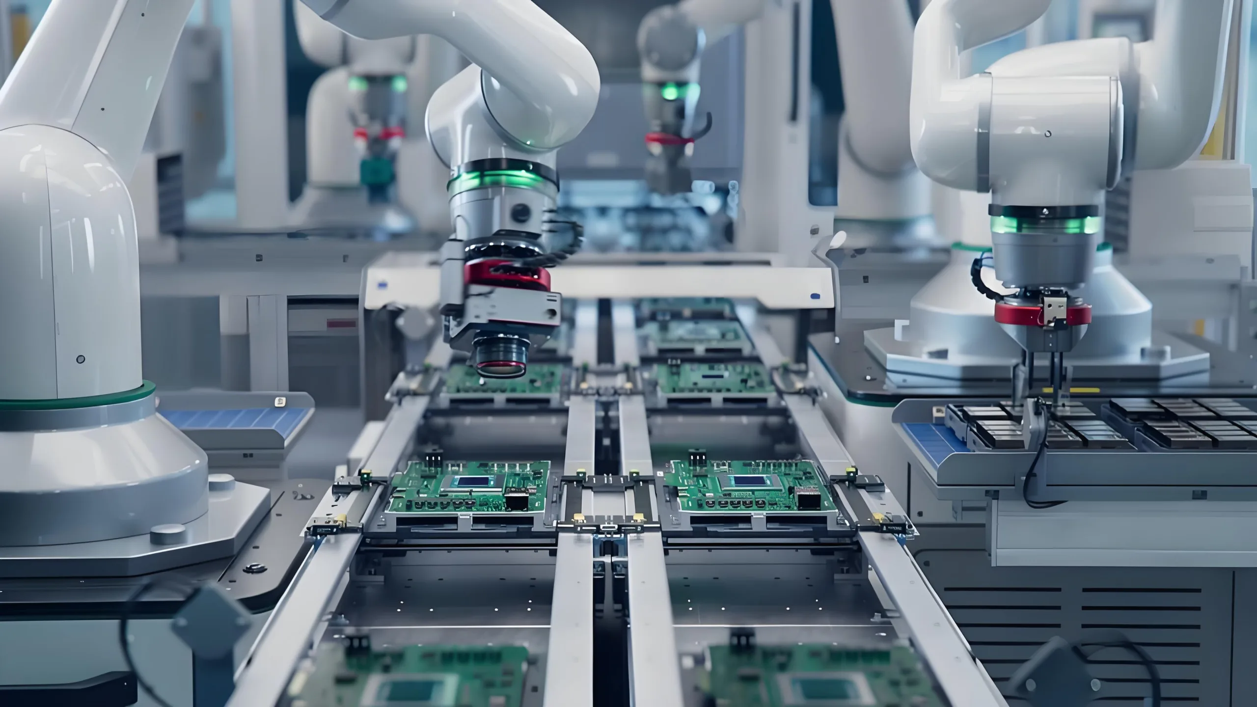
Precision Equipment: Utilizes fully automated Ldi exposure machines (±1.5μm accuracy) and vacuum etching lines (1.5/1.5 Lățimea/distanțarea liniei mil).
-
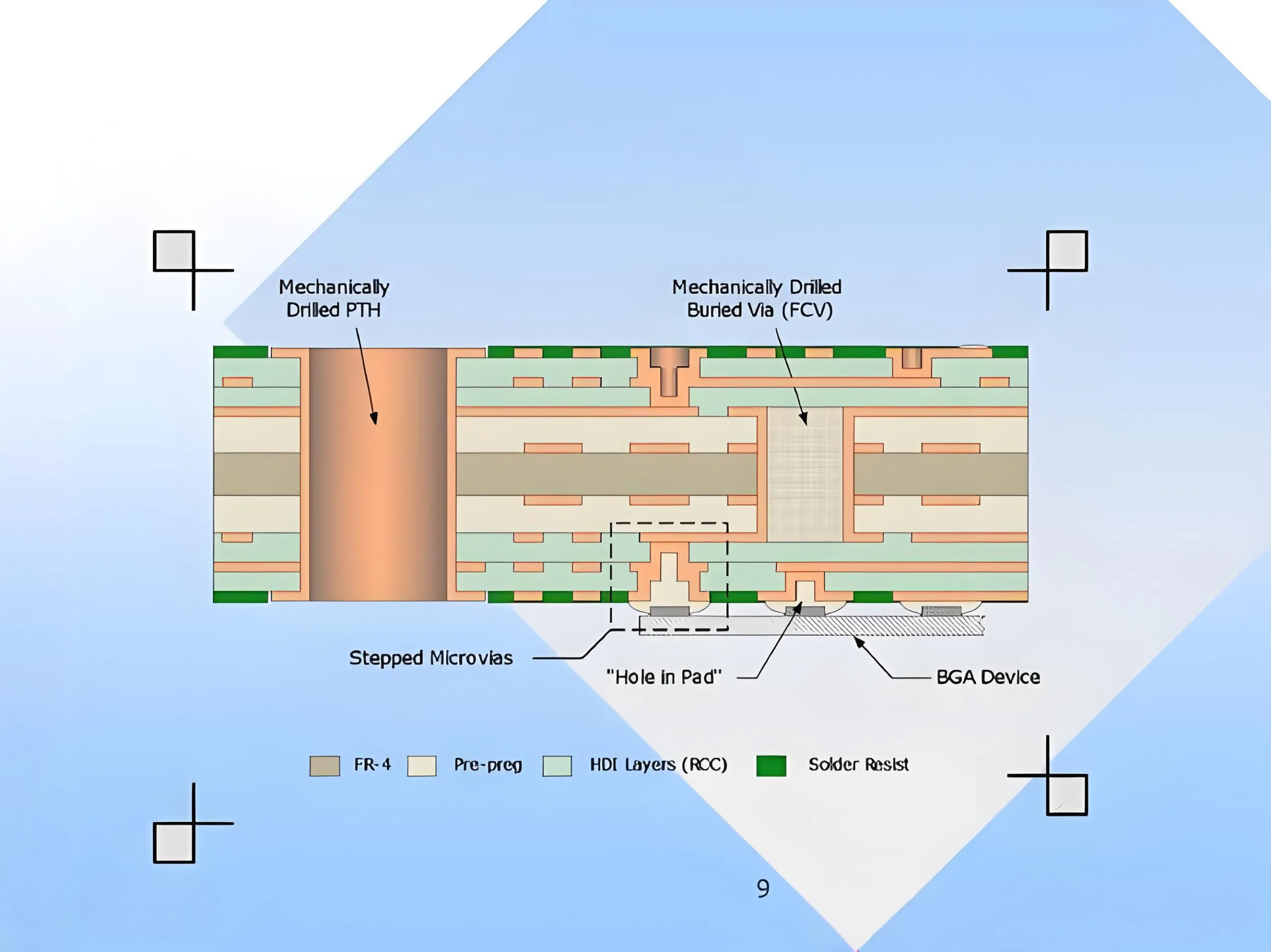
Multilayer PCB Technology: Suport 1-100 layer boards with interlayer alignment tolerance ≤15μm (Formula: δ = k√(n), where n = layer count, k = process constant).
-
Material Versatility: Rogers, FR4, aluminum-based PCBs, etc., meeting high-temperature demands (Tg 180°C-220°C) for automotive/aerospace applications.
2. 24-Hour Rapid PCB Prototyping Service
-
Global Fastest Delivery: 24 hours for 2-layer, 72 hours for 6-layer boards (industry average: 5-7 zile).
-
Zero Startup Cost: Accepts orders from 1 piece with free DFM engineering review.
-
Success Story: Reduced new product development cycle by 60% for a German industrial client.
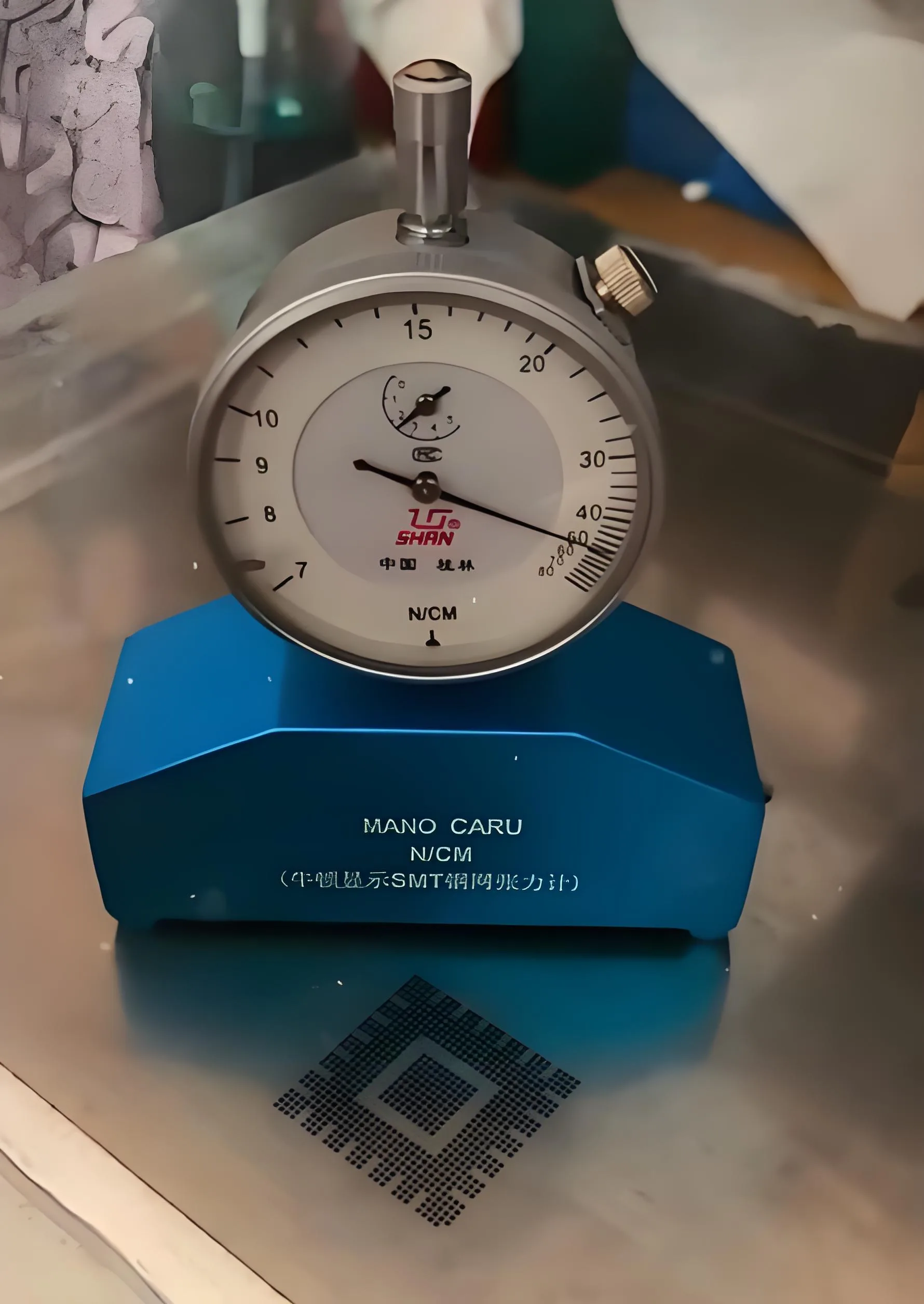
3. Laser Stencil Core Technology
-
Tension Control: 35±5 N/cm² (IPC-7525 compliant).
-
Nano Coating: Extends lifespan to 500,000 print cycles.
-
Smart Inspection: AOI systems detect aperture defects ≥15μm.
Scientific Manufacturing: Data-Driven PCB Process Innovation
Key Process Control Points (Real Data)
| Parametru | UGPCB Standard | Industry Benchmark |
|---|---|---|
| Copper Thickness Uniformity | ±1.5μm | ±5μm |
| Controlul impedanței | ± 5% | ±10% |
| Hole Position Accuracy | ±25μm | ±50μm |
Defect Prevention (Solving User Pain Points)
-
Pad Overlap Issues: Dynamic drilling compensation algorithm used (Compensation Δd = 0.85 × Tool Wear Rate).
-
Silkscreen Imperfections: Enforced DFM rule checks (Font ≥40mil, Distance to Pad >10mil).
End-to-End Service: From Design to Delivery
File Specifications (Improving First-Pass Yield)
-
Accepts Gerber/ODB++/PCB source files.
-
Free one-stop solutions for common PCB design and manufacturing challenges. https://www.ugpcb.com/capacity/download/
Quality Certification System
-
Dual-Standard Inspection: UGPCB Level 2 + Clasa IPC 3.
-
Echipament de testare: Flying Probe Tester (0.1mm min. pitch), 3D X-ray (BGA inspection).

Luați măsuri acum: Obțineți soluția dvs. PCB personalizată
Limited-Time Offer: Submit Gerber files → Receive Quote + Stencil Design within 24 ore.
-
Contact: sales@ugpcb.com / Online Quotation System
-
Key Solutions: PCB Bulk Manufacturing Supplier | Rush Prototype Service | High-Precision Stencil Fabrication
WeChat
Scanați codul QR cu WeChat