
UGPCB’s PCB Prototyping Capability: The Technology Innovation & Industry Benchmark Behind 72-Hour Rapid Delivery
PCB (Placă de circuit tipărită) serves as the “skeleton” şi “sistemul nervos” of modern electronics, acting as the core carrier connecting all electronic components. From smartphones to satellite communications, medical devices to autonomous driving systems, peste 99% of electronic devices rely on the stable operation of high-performance PCBs. In the fierce competition of product development, rapid, de încredere, and high-quality PCB prototyping services have become a decisive factor for companies aiming to seize market opportunities. Leveraging deep technical expertise and an advanced manufacturing system, UGPCB is redefining industry standards for quick-turn Fabricarea PCB.
🔍 I. Prototiparea PCB: The Cornerstone and Litmus Test of Electronic Innovation
The evolution of PCBs spans over 130 ani. From early manual wiring to today’s Interconectare de înaltă densitate (HDI) şi Substraturi IC, its development has progressed in lockstep with electronic technology revolutions. The practical application of Copper-Clad Laminate (Ccl) technology during WWII was a pivotal turning point, replacing complex and error-prone manual wire soldering and laying the foundation for the reliability, stabilitate, and miniaturization of modern electronics.
-
Engineer’s Challenge: Committing a PCB design with unresolved flaws to mass production leads to catastrophic consequences – performance failures, costly recalls, project delays, customer loss, and brand reputation damage.
-
UGPCB Solution: Providing comprehensive, high-precision, and rapid-response Design PCB şi PCB prototyping services is the first and most critical safeguard for engineers transforming innovative concepts into reliable products.
-
💡 Professional Insight: The core value of PCB prototyping lies in “early detection, early correction.” Statistics show that fixing errors during the prototype phase costs merely 1/100th (sau mai putin) of the cost incurred during mass production. UGPCB rapid PCB prototyping capability is key to significantly saving clients R&D costs and time.
🛠️ II. Deep Dive: UGPCB’s Core Technical Capabilities in PCB Prototyping
UGPCB’s manufacturing capabilities cover everything from basic single/double-sided boards to cutting-edge IC packaging substrates, featuring stringent parameters and industry-leading processes.
📊 1. Core Process Parameters & Technical Specifications (UGPCB PCB Prototyping Capabilities Overview)
-
Key Data:
-
Board Thickness Range: Single/Double: 0.10mm – 8.0mm (4 mil – 315 mil); Multilayer: 0.15mm – 8.0mm (6 mil – 315 mil)
-
Min. Finished Size: 0.5 x 1.0mm (Extreme Miniaturization Capability)
-
Max. Straturi: Standard: Up to 100 straturi (Requires Review); Hybrid RF: 4-32 straturi
-
High-Frequency/Special Materiale: Rogers®, Arlon®, Taconic®, Isola® (FR408, 370HR), Teflon®/PTFE, ceramică, Hydrocarbon Ceramic, Materiale hibride
-
📡 2. High-Frequency & High-Speed PCB Prototyping: Key to Dominating the GHz Era
Driven by the surge in 5G/6G, radar, satellite communication (frecvențe >1GHz), and AI computing demands, high-frequency high-speed PCBs are the technological high ground. The core challenge lies in controlling signal loss and maintaining impedance stability.
-
Provocări tehnice: Stability of Dielectric Constant (DK) & Tangenta de pierdere (Df), copper foil surface roughness, precise dielectric layer thickness control.
-
UGPCB Advantages:
-
Material Expertise: Proven processing of top high-frequency laminates like Rogers® (RO3000™, RO4000® series), Arlon® (AD/CL series), Taconic® (RF-35, TLY series), Isola® (FR408HR, Astra™).
-
Controlul impedanței: Strict tolerance control within ±5%, often ±3%, meeting the most demanding signal integrity cerințe.
-
Aplicații: mmWave radar, satellite communication payloads, high-speed networking equipment (400G/800G), high-end test instruments.
-
-
📐 Technical Formula – Characteristic Impedance (Microstrip Simplified Model):
Z₀ ≈ (87 / √(εr + 1.41)) * ln(5.98h / (0.8w + t))-
Z₀: Target Impedance (Oh) -
εr: Substrate Material Relative Dielectric Constant -
h: Grosime dielectrică (mil) -
w: Trace Width (mil) -
t: Trace Thickness (mil) -
UGPCB engineers utilize precise calculations and simulation to ensure high-frequency circuit impedance accurately matches design values.
-
🔄 3. Rigid-Flex PCB Prototyping: The Perfect Enabler for Complex 3D Designs
Rigid-flex PCBs combine the stable support of rigid boards with the dynamic bending capability of flexible circuits, offering a revolutionary solution for device miniaturization, weight reduction, and enhanced reliability.
-
Unique Advantages:
-
Significantly reduces connectors and cables, improving system reliability (fewer failure points).
-
Freely adapts to complex 3D spaces, optimizing internal device layout.
-
Reduces overall weight and volume, ideal for wearable devices, aerospațial, şi precision medical instruments.
-
-
Provocări & UGPCB Breakthroughs:
-
Traditional Pain Points: Complex processes (până la 50+ steps), high material costs, yield control difficulties, long production cycles.
-
UGPCB Solution: Optimizing material selection (De ex., PI coverlay/adhesive matching), employing high-precision lamination and laser drilling, implementing strict process control (per IPC-2223B, 6013D standards), effectively boosting yield and shortening prototype lead times.
-
🧩 4. High-Layer-Count PCBs & IC Substrate Prototyping: Enabling High-Density Integration
Increasingly powerful electronics drive PCBs towards high-layer-count (>10 straturi), ultra-high-density routing, and advanced packaging. Substraturi IC, acting as the “interpreter” between chips and motherboards, present extremely high technical barriers.
-
Multilayer Trends: Continuously shrinking line width/space (L/S down to ≤50μm/50μm), higher precision for microvias (<100μm), stricter layer-to-layer alignment.
-
Substrat IC – The Core of Packaging:
-
Definiţie: High-end PCBs directly mounting the chip (Die), providing electrical interconnection, Managementul termic, and physical protection.
-
Key Characteristics: Ultra-high-density routing (HDI/SLP technology), ultra-thin cores (<100μm possible), fine lines (L/S down to 20μm/20μm), high surface flatness, excellent thermal management.
-
UGPCB Strength: Possesses mature BGA (Ball Grid Array) şi eMMC (Embedded MultiMediaCard) substrat prototyping and low-to-medium volume production capabilities, supporting client R&D in processors, memorie, AI accelerator chips, și mai mult.
-
⏱️ III. Speed & Cost Advantage: UGPCB’s Core Competitiveness in PCB Prototyping
In the electronics market where “speed is paramount,” prototyping velocity directly impacts timp la piață (TTM). Simultan, effective cost control is crucial for R&D budgets.
-
Livrare rapidă: UGPCB optimizes production flow and supply chain management. Standard PCB prototype lead times can be compressed to an impressive 72 ore (3 zile). Complex boards (De ex., RF, HDI, rigid-flex, >20 straturi) typically complete within 1-2 săptămâni (depending on complexity), far exceeding industry averages.
-
Low-Cost Prototyping Strategy:
-
Efficient Design Validation: Uses proven cost-effective materials and standardized processes for rapid functional verification.
-
Flexible Solutions: Recommends the most cost-effective material and process combinations based on testing needs (Performanță electrică, mechanical fit, basic function).
-
Value Proposition: Early prototype validation can prevent up to 90% of potential losses during mass production. UGPCB low-cost PCB prototyping is the smart choice for managing R&D risk.
-
📌 Call to Action: Seeking PCB prototyping services that combine speed, fiabilitate, and cost advantage? Contact UGPCB NOW for a custom quote! We offer free DFM (Proiectare pentru producție) analysis to optimize your design and accelerate product launch! [Click the live chat tool at the bottom right for free technical support]
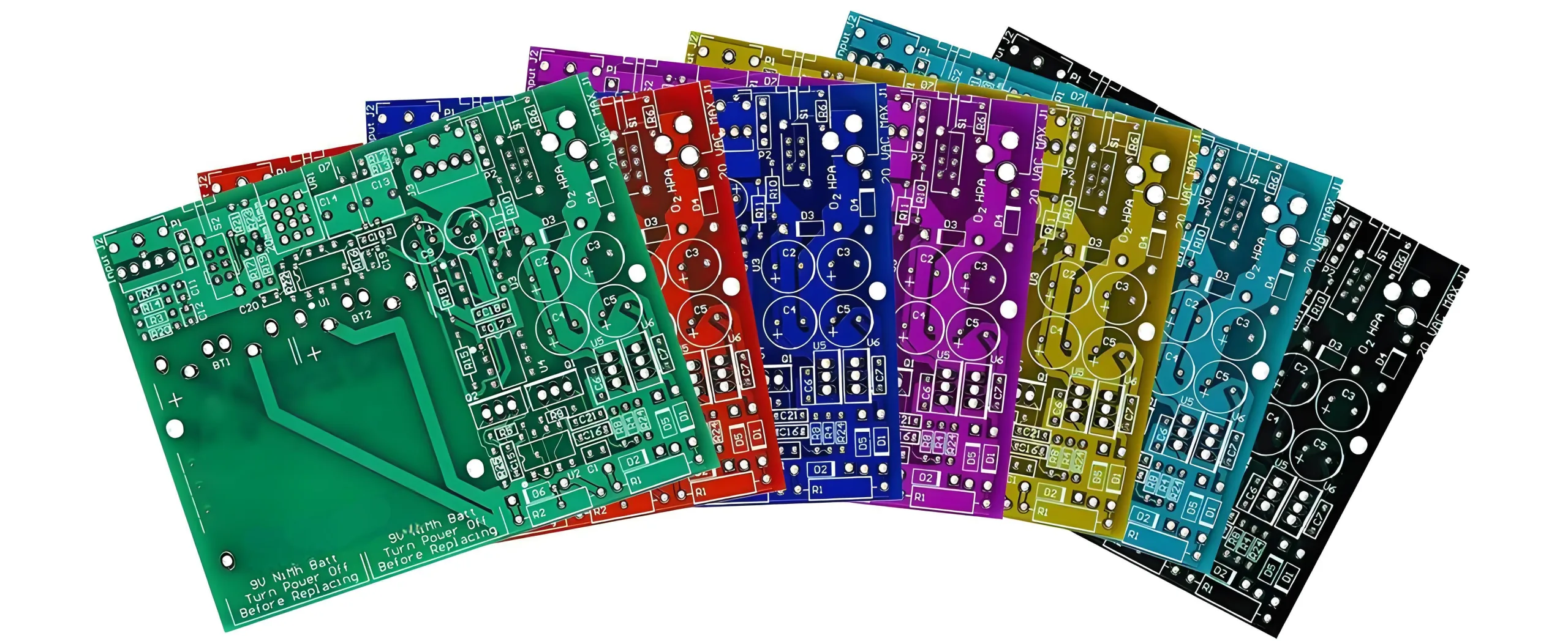
🎨 IV. Beyond Green: The Science and Art of PCB Color Selection
în timp ce “engineering green” is the classic PCB look, solder mask colors offer far more variety. UGPCB provides options like blue, galben, roşu, negru, and white – driven not just by aesthetics, but also functionality:
-
White PCBs: High reflectivity, significantly enhances light efficiency and uniformity in LED lighting applications.
-
Black PCBs: Low reflectivity, reduces stray light interference, ideal for stage equipment, high-end AV products, conveying a low-key professional feel.
-
Inspecţie & Rework: High contrast between light backgrounds (galben, alb) and dark traces (verde, blue) facilitates visual inspection and manual repair.
-
Brand Identity: Custom colors strengthen product visual identity and brand image.
🚀 V. From Design to Mass Production: UGPCB’s End-to-End PCB Solution Value Loop
UGPCB’s value extends far beyond bare board manufacturing, encompassing the entire product lifecycle:
-
Design Support & Prototype Validation (Valoarea de bază): Quick-turn prototyping provides the golden window to find and fix design flaws, ensuring a robust foundation.
-
Function & Performance Testing: Engineers use prototypes for signal integrity (SI), Integritatea puterii (Pi), thermal simulation, environmental stress testing, etc., verifying product performance under various conditions.
-
Marketing & Demo Powerhouse: Fully functional PCB prototypes are ideal for exhibitions, client demos, and funding pitches, tangibly showcasing product value.
-
Seamless Ramp to Production: UGPCB’s prototyping processes align closely with mass production lines, ensuring consistent performance and mitigating transition risks.
-
PCB (Asamblare) Prototyping Services: Offers full PCBA prototyping inclusiv component sourcing (BOM), ansamblu SMT, THT (DIP) assembly, and testing. Delivering ready-to-run functional modules drastically accelerates final product development and shortens time-to-market.
💎 Conclusion: Choose UGPCB, Choose an Innovation Accelerator
In the fast-paced electronics industry, time is market share, and quality is paramount. UGPCB, with its:
-
Cutting-edge process capabilities (covering RF/high-speed, rigid-flex, high-layer-count, substraturi IC),
-
Extreme delivery speed (fastest 72 ore),
-
Flexible cost strategies (low-cost validation options),
-
Rigorous quality systems (complying with IPC, etc.),
-
Comprehensive service chain (design support, PCB prototyping, Ansamblu PCBA),
has become the trusted Prototip PCB and volume manufacturing partner for global engineers and R&D teams. Whether in consumer electronics, electronice auto, dispozitive medicale, control industrial, aerospațial, or communications, UGPCB provides a solid, rapid, and high-quality physical foundation for your innovation.
Luați măsuri acum!
-
Get Your Custom PCB Prototype Quote
-
Consult an Expert: Our technical team is ready to answer your questions on high-frequency design, rigid-flex structures, controlul impedanței, selecția materialului, și mai mult.
-
Explore More Capabilities:
Choose UGPCB – Let us be your powerful partner on the road to success!
WeChat
Scanați codul QR cu WeChat