

EMC (ความเข้ากันได้ทางแม่เหล็กไฟฟ้า) design is to พีซีบี engineers what battlefield tactics are to military commanders – a single misstep can cost the entire campaign. In today’s era of high-speed digital systems and mixed RF circuits, เกิน 85% of radiated emission failures trace back to PCB-level deficiencies in filtering, discontinuous shielding structures, or incorrect grounding strategies. EMC problems are never isolated faults; they are systemic breakdowns.
EMC design ultimately operates on three dimensions: shielding, filtering, and grounding – shielding traps interference inside a cage, filtering blocks interference on the lines, and grounding gives interference a path to escape. These three elements form a castle’s defense system: shielding is the wall, filtering is the gate, and grounding is the moat. A thick wall is useless if the gate stands open; a sturdy gate is worthless without a moat.
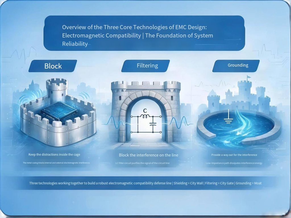
บท 1: Shielding – Trapping Interference in a Cage
1.1 The Essence of Shielding
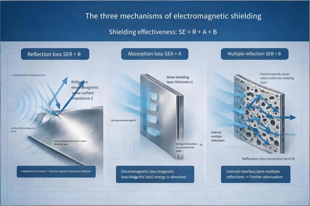
Shielding uses conductive or magnetic materials to form an enclosed surface. This surface confines electromagnetic fields within a defined region or prevents external fields from entering. Shielding addressesspatial coupling – namely capacitive coupling, inductive coupling, and radiative coupling.
When an electromagnetic wave encounters a shield, three phenomena occur:
| Mechanism | หลักการ | Key Influencing Factors |
|---|---|---|
| Reflection loss (R) | Wave reflection at the shield surface due to impedance mismatch | Material conductivity, wave impedance mismatch |
| Absorption loss (อัน) | Wave energy converted to heat during penetration | Material conductivity, permeability, ความหนา |
| Multiple reflections (ข) | Repeated internal reflections within the shield | Shield thickness, internal structure |
Total shielding effectiveness: SE = R + อัน + ข (DB)
Absorption loss A can be calculated asเอ = 8.69 × (t/δ), where t is shield thickness and δ is skin depth. This meansone skin depth of shielding material provides approximately 9 dB of absorption loss; doubling the thickness adds another 9 DB.
1.2 Electric Field Shielding vs. Magnetic Field Shielding
| การเปรียบเทียบ | Electric Field Shielding | Magnetic Field Shielding |
|---|---|---|
| Interference source | ไฟฟ้าแรงสูง, low current | High current, low voltage |
| การเลือกวัสดุ | การนำไฟฟ้าสูง (ทองแดง, อลูมิเนียม) | High permeability (เหล็ก, Mu-metal) |
| หลักการ | Reflects electric field, creates opposing field | Channels magnetic flux, concentrates it inside |
| Grounding requirement | Must be grounded | Not mandatory |
| Thickness requirement | Thin suffices (ผลกระทบต่อผิวหนัง) | Requires sufficient thickness |
1.3 Five Critical Shielding Design Rules
- การเลือกวัสดุ: Use copper or aluminum for electric fields and far-field; use ferromagnetic materials for low-frequency magnetic fields.
- Seam control: Keep seam lengths below λ/20; use conductive gaskets.
- Aperture control: Keep hole dimensions below λ/20; minimize the number of openings.
- Cable penetration: Use filtered connectors or shielded adapters at penetration points.
- Grounding: The shield must be well grounded; มิฉะนั้น, it becomes an antenna.
Shielding has limitations. Low-frequency magnetic fields are extremely difficult to shield (requiring thick ferromagnetic materials). Apertures and seams severely degrade performance. Shielding is expensive, heavy, and complex to manufacture.Shielding is the last line of defense – prioritize source control and filtering first.
บท 2: Filtering – Blocking Interference on the Lines
2.1 The Essence of Filtering
Filtering inserts a frequency-selective network into the signal path. This network passes desired signals while blocking interference. Filtering addressesconducted coupling – interference that propagates through cables.
Low-pass filters are the most common type in EMC applications because most interference is high-frequency while useful power and signals are low-frequency.
2.2 The Power EMI Filter – The Classic EMC Filter
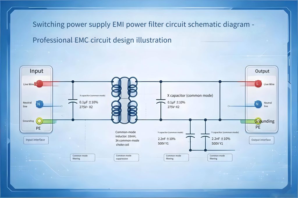
The power EMI filter is standard equipment for switch-mode power supplies. Its typical structure consists of X capacitors, Y capacitors, and common-mode chokes connected between the live, neutral, and ground lines.
| ส่วนประกอบ | Suppression Mode | Typical Parameters |
|---|---|---|
| X capacitor | Differential-mode interference | 0.1–2.2 μF |
| Y capacitor | Common-mode interference | 1–4.7 nF |
| Common-mode choke | Common-mode interference | 1–10 mH |
| Differential-mode inductor | Differential-mode interference | Tens to hundreds of μH |
2.3 The Core Metric: การสูญเสียการแทรก
การสูญเสียการแทรก (อิลลินอยส์) is the key parameter for evaluating filter performance. It is defined as the ratio of load-side voltage before and after filter insertion:
IL = 20log₁₀(V₁/V₂) (DB)
ต่อCISPR 17:2011, which specifies methods to measure the radio interference suppression characteristics of passive EMC filtering devices, a quality DC power filter should achievecommon-mode insertion loss ≥ 40 dB and differential-mode insertion loss ≥ 30 DB across the 150 kHz – 30 MHz conducted emission band. CISPR 17 defines test configurations including 50Ω/50Ω symmetrical (differential mode) and asymmetrical (common mode) measurements, as well as non-50Ω systems such as 0.1Ω/100Ω and 100Ω/0.1Ω topologies.
2.4 Four Filter Design Principles
- Common mode first, then differential mode: Common-mode interference is typically harder to handle; prioritize common-mode filter design.
- Place close to the source: Locate the filter as close as possible to the interference source or the sensitive port.
- Mind impedance matching: The filter operates between source impedance and load impedance; impedance mismatch severely degrades performance. Per CISPR 17, asymmetric impedance testing (เช่น, 0.1Ω/100Ω) should be used to verify filter performance under worst-case conditions.
- Ground well: The common terminal of Y capacitors and the filter must connect to ground with low impedance.
บท 3: Grounding – Giving Interference a Path to Escape
3.1 The Essence of Grounding
Grounding serves two core purposes: safety grounding (protecting personnel by providing a fault current path) และsignal grounding (providing a reference potential for circuits and a low-impedance return path for interference currents). EMC focuses primarily on signal grounding.
Grounding addresses theloop problem – interference currents need a low-impedance return path. Poor grounding forces interference currents through unintended paths, creating coupling.
3.2 Ground Impedance – Inductance Dominates at High Frequencies
The impedance of a PCB trace or wire includes resistance R and inductive reactance XL:
Z = R + jXL = R + j2πfL
Consider a PCB trace 10 cm long, 1.5 mm wide, และ 50 หนา ไมครอน:
- ความต้านทาน: R = ρL/s = 0.02 × 0.1 / (1.5 × 0.05) data 0.026 โอ้
- Inductance: ประมาณ0.08 μH (0.8 μH/m self-inductance)
- ที่ 1 เมกะเฮิรตซ์, inductive reactance: XL = 2π × 1×10⁶ × 0.08×10⁻⁶ ≈ 0.5 โอ้ -19 times the resistance!
Key conclusion: ที่ความถี่สูง, inductance dominates impedance.Shortening the ground path is the most effective way to reduce impedance. A solid ground plane offers the lowest impedance. Flat conductors (ฟอยล์ทองแดง) have lower high-frequency impedance than round conductors (ลวด).
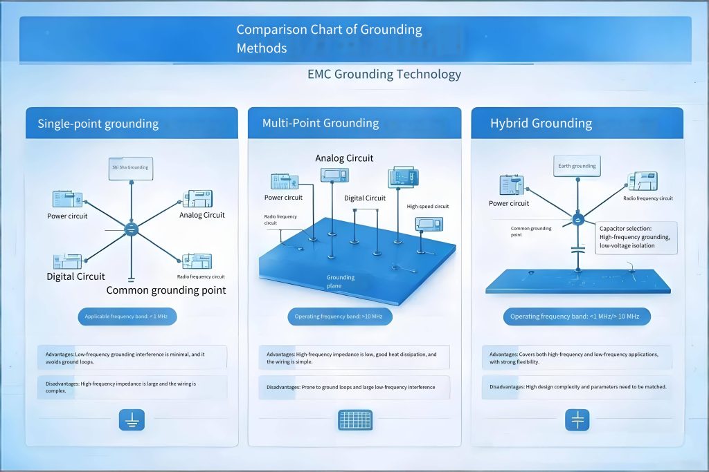
3.3 Three Grounding Methods
| Grounding Method | หลักการ | ช่วงความถี่ | ข้อได้เปรียบ | Disadvantage |
|---|---|---|---|---|
| Single-point grounding | All ground points connect to one point | <1 เมกะเฮิรตซ์ | No ground loops | High impedance at high frequencies |
| Multi-point grounding | Each ground point connects locally to ground plane | >10 เมกะเฮิรตซ์ | Low high-frequency impedance | Ground loops possible |
| Hybrid grounding | Single-point at low frequencies, multi-point at high frequencies | Broadband | Balances low and high frequencies | Complex design |
In practice, most products contain both low-frequency and high-frequency circuits.Hybrid grounding is the mainstream engineering approach – single-point grounding for low-frequency sections (avoiding ground loops) and multi-point grounding for high-frequency sections (reducing impedance). Capacitors and inductors enable “frequency-selective grounding.”
3.4 The Solid Ground Plane Advantage
A solid ground plane provides a low-impedance return path for current, reduces noise, and improves circuit reliability. On multilayer boards, dedicating large areas of the PCB to ground and connecting components along the shortest possible routes minimizes ground impedance. A continuous ground plane acts as a shield underneath high-speed or sensitive traces, absorbs stray electromagnetic fields, ลดการครอสทอล์ค, and improves EMC performance.
บท 4: Three-Way Synergy – 1+1+1 > 3
4.1 Why Synergy Is Essential
Each technique – shielding, filtering, and grounding – has limitations when used alone. But when they work together, the effect multiplies:
| สถานการณ์ | ผล |
|---|---|
| Shield not grounded | Nearly useless; the shield becomes a secondary radiator |
| Filter not grounded | High-frequency filtering fails |
| Poor grounding system | Shield becomes antenna; filter becomes coupling path |
| All three working together | Maximum effectiveness |
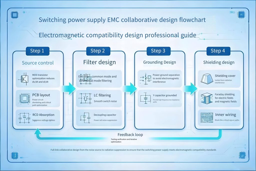
4.2 กรณีศึกษา: Switch-Mode Power Supply EMC Design
ขั้นตอน 1 – Source control: Optimize MOSFET gate drive (reduce switching slew rate). Optimize เค้าโครง PCB (minimize power loop area). Add RCD snubber circuits.Reducing the power loop area by 50% can lower radiated emissions by approximately 12 DB.
ขั้นตอน 2 – Filter design: Install X capacitors, common-mode chokes, and Y capacitors at the input (power EMI filter). Add an LC filter at the output. Place decoupling capacitors at the control IC power pins.
ขั้นตอน 3 – Grounding design: Separate power ground from signal ground; connect them at a single point. Ground Y capacitors locally to the chassis. Ground the heatsink.
ขั้นตอน 4 – Shielding design: Add shielding cans over MOSFETs and rectifiers. Add a Faraday shield layer to the transformer. Route critical signals on inner layers with ground planes on both sides.
4.3 กรณีศึกษา: High-Speed Digital Board EMC Design
ขั้นตอน 1 – Source control: Control signal rise times (series termination resistors). Keep clock traces away from I/O connectors. Route differential pairs symmetrically.
ขั้นตอน 2 – Grounding design: Maintain a solid ground plane; avoid splits. Dedicate a separate ground plane section for the I/O area and connect it to the chassis.
ขั้นตอน 3 – Filter design: Add common-mode chokes on I/O lines. Use π-type filters at the power entry point. Place decoupling capacitors at every IC power pin.In a standard six-layer board stack-up, solid ground planes on layers 2 และ 5 provide 15–25 dB of radiation suppression across the 30 เมกะเฮิรตซ์ – 1 GHz band.
ขั้นตอน 4 – Shielding design: Use shielded I/O connectors. Apply conductive gaskets at chassis seams. Route critical signals on inner layers.
บท 5: Design Priority – Source Control Always Comes First
5.1 The Five-Layer Defense
| ชั้น | Measure | Effect | ค่าใช้จ่าย |
|---|---|---|---|
| ชั้น 1 | Source control (component selection, layout optimization) | Fundamental solution | ต่ำสุด |
| ชั้น 2 | Loop design (minimize loop area, การจับคู่ความต้านทาน) | Significant improvement | ต่ำ |
| ชั้น 3 | การกรอง | Effective suppression | ปานกลาง |
| ชั้น 4 | Grounding | Systematic improvement | ปานกลาง |
| ชั้น 5 | Shielding | Last-resort solution | สูงสุด |
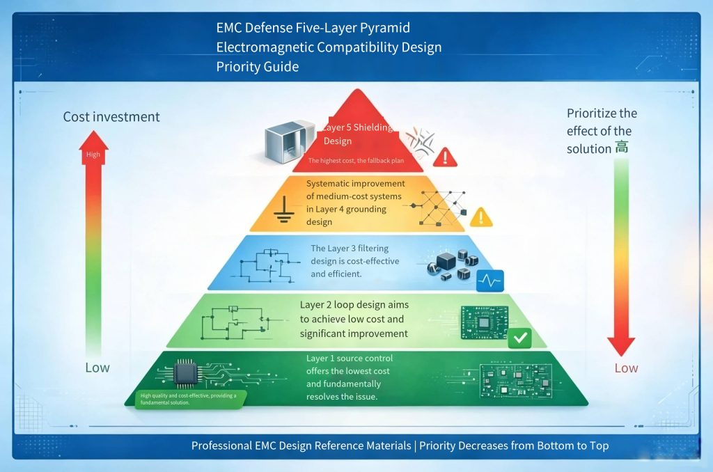
Core principle: Solve at the source whenever possible; filter only what you cannot eliminate at the source; shield only as a last resort.
5.2 Why Source Control Matters Most
| การเปรียบเทียบ | การควบคุมแหล่งที่มา | Remedial Measures (Filtering/Shielding) |
|---|---|---|
| Effect | Fundamental | Symptom treatment |
| ค่าใช้จ่าย | Nearly zero | Requires additional components/materials |
| ความน่าเชื่อถือ | สูง | May degrade with temperature/aging |
| เสรีภาพในการออกแบบ | สูง | Constrained by space and cost |
| Production consistency | ดี | Affected by component tolerances |
Reducing MOSFET switching speed by 30% can lower high-frequency noise by 6–10 dB – more effective than any filter.
บท 6: EMC Design Checklist – Quick Reference
Schematic Stage
- □ Power input has an EMI filter; every IC power pin has a decoupling capacitor
- □ High-speed signals have termination resistors
- □ I/O lines have TVS/ESD protection
- □ Clocks have RC filtering or spread spectrum
- □ Isolation between high-voltage and low-voltage sections meets IPC-2221 requirements
PCB Layout Stage
- □ Power loop area minimized; power devices placed close together
- □ Analog/digital/power/RF sections partitioned
- □ I/O connectors grouped together and placed away from noise sources
- □ Clock traces kept away from I/O; routed on inner layers with ground planes on both sides
- □Ground plane kept solid; avoid splits
Mechanical/Structural Stage
- □ Shielding cans added over critical noise sources; shield grounding resistance ≤ 0.1 โอ้
- □ Seams treated with conductive gaskets; gap length < λ/20
- □ Shielded cables and connectors used
- □ Shield, PCB ground, and chassis ground connected with low impedance
- □ Ventilation holes kept below λ/20; use waveguide vents when necessary
บทสรุป: EMC Design Is Systems Engineering
EMC design is not about point solutions – it is aboutsystems engineering.
Shielding, filtering, and grounding form an inseparable trio.
But remember the core principle: source control comes first, filtering provides midfield support, shielding is the last line of defense, and grounding is the foundation that runs through everything.
When you face those dancing emission spikes on the spectrum analyzer in the EMC lab, trace them back to the decisions made on your การออกแบบ PCB drawings – every choice about placement, การกำหนดเส้นทาง, การแยกส่วน, การต่อสายดิน, and shielding – those are the choices that truly determine success or failure.
EMC is not measured into a product; it is designed into it.
คำชี้แจงแหล่งข้อมูล:
The technical data and standards cited in this article are based on the following sources:
- The shielding effectiveness formula SE = R + อัน + B and the absorption loss formula A = 8.69 × (t/δ) are referenced from electromagnetic shielding theory literature.
- The insertion loss definition IL = 20log₁₀(V₁/V₂) and the CISPR 17:2011 ข้อกำหนดมาตรฐาน (common-mode ≥40 dB, differential-mode ≥30 dB across the 150 kHz–30 MHz band) are referenced from CISPR 17:2011 -Methods of measurement of the suppression characteristics of passive EMC filtering devices.
- PCB trace impedance calculations R = ρL/s and inductive reactance XL = 2πfL are referenced from PCB grounding and interference suppression technical literature.
- PCB-level EMC data (85% of radiated emission failures trace to PCB-level issues; six-layer board ground plane suppression of 15–25 dB) are referenced from EMC troubleshooting and practical design literature.
- The IPC-2221 standard framework for PCB electrical requirements (การต่อสายดิน, shielding, ความสมบูรณ์ของสัญญาณ) is referenced from IPC-2221 –มาตรฐานทั่วไปเกี่ยวกับการออกแบบแผ่นพิมพ์.
- UL PCB safety standards (อล 796 for rigid printed wiring boards) are referenced from UL 796 -Standard for Printed-Wiring Boards.
