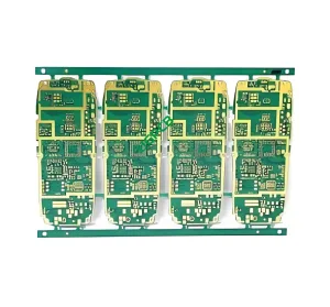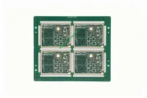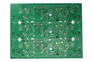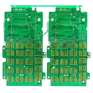
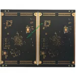
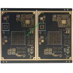
1. ภาพรวมผลิตภัณฑ์: What Is a 10-Layer 1-Level HDI PCB?
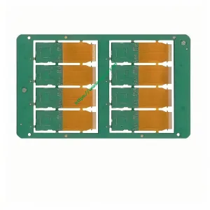
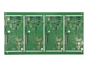
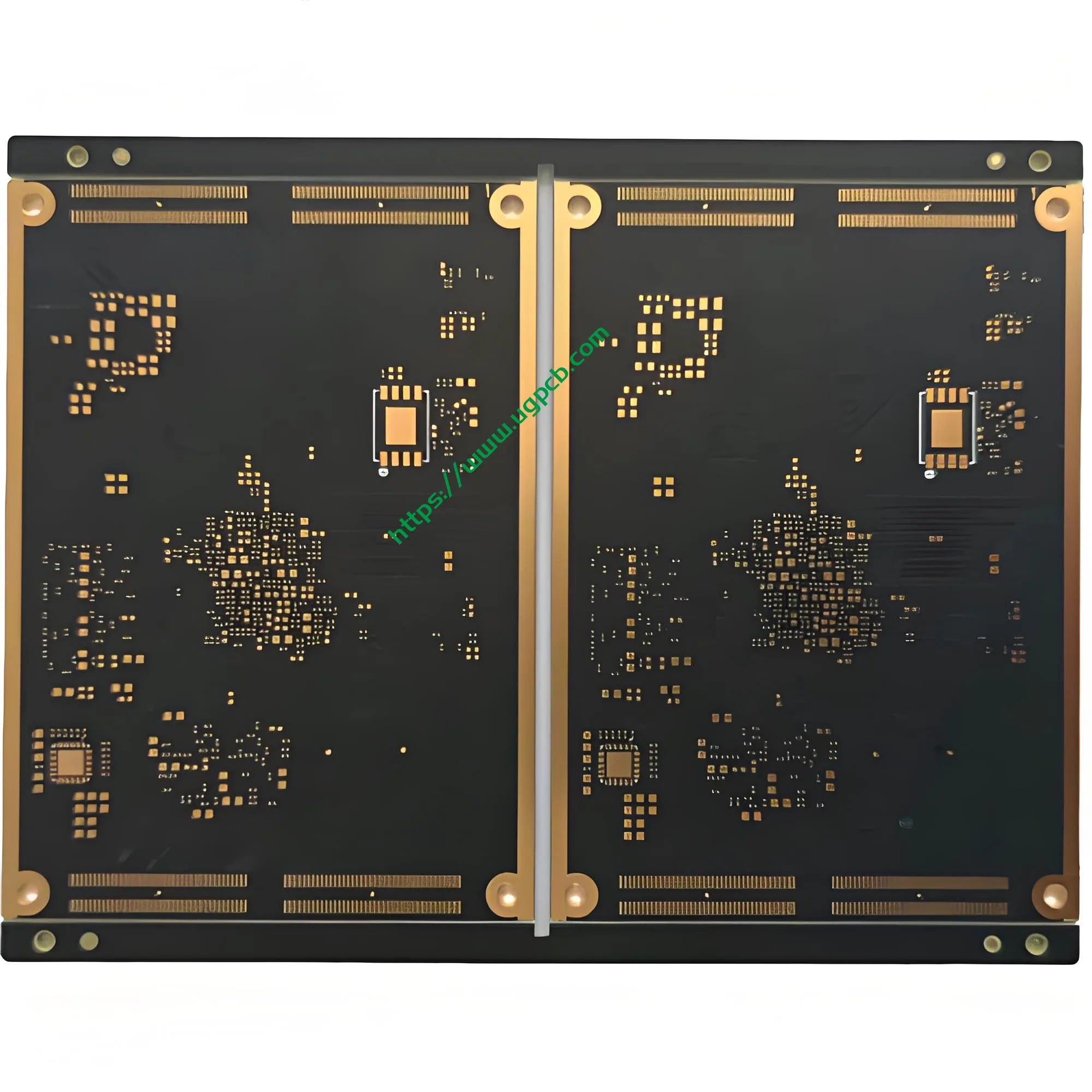
A 10-layer 1-level HDI PCB is a high-density interconnect printed circuit board. It uses a 1+8+1 กองซ้อน. The board has an 8-layer core. Each side receives one build-up layer. Laser-drilled microvias connect the outer layers to the inner layers.
IPC-2226A places this design in Type I HDI. Type I HDI has one microvia layer on each side of the core. The standard defines a microvia as a blind via with a maximum aspect ratio of 1:1. Its total depth must not exceed 0.25 มม.
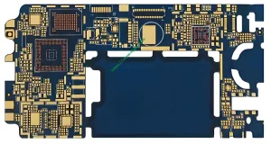
This 10-layer HDI PCB packs more routing density into less space. It suits smartphones, อุปกรณ์อิเล็กทรอนิกส์ยานยนต์, อุปกรณ์การแพทย์, and AI servers. It also supports advanced พีซีบี designs that need fine-pitch ส่วนประกอบ.

2. Core Parameters and Technical Specifications
UGPCB’s 10-layer 1-level HDI PCB offers the following key specifications:
| พารามิเตอร์ | ข้อมูลจำเพาะ |
|---|---|
| เลเยอร์ | 10 ชั้น |
| HDI level | 1-ระดับ (1+8+1) |
| ลามิเนต | FR4 Tg170 |
| ความหนาของบอร์ด | 1.6 มม |
| ขนาดแผง | 121.6 × 95 มม (2-ขึ้น) |
| ความหนาของทองแดงภายนอก | 1 ออนซ์ (35 μm) |
| ความหนาของทองแดงชั้นใน | 1 ออนซ์ (35 μm) |
| ขั้นต่ำผ่านหลุม | 0.20 มม |
| รูบอดขั้นต่ำ | 0.10 มม (laser-drilled) |
| Minimum BGA pitch | 0.25 มม |
| ความกว้าง/ระยะห่างขั้นต่ำของเส้น | 3/2.7 MIL (0.076/0.069 มม) |
Laminate selection basis: FR4 Tg170 is a high-Tg epoxy glass laminate. It meets IPC-4101C requirements. อุณหภูมิการเปลี่ยนสถานะคล้ายแก้ว (ทีจี) is at least 170°C. Its decomposition temperature (TD) is about 350°C. Its Z-axis CTE ranges from 45 ถึง 55 ppm/° C. IPC-4101C sets the upper CTE limit at 60 ppm/° C.
This high-Tg material improves thermal stability during lead-free soldering. Lead-free reflow peaks usually reach 245–260°C. IPC-4101 groups high-Tg FR-4 from 170–180°C for automotive and high-temperature applications.
Precision design basis: ที่ 0.10 mm laser blind via meets the IPC-2226A microvia definition. That definition covers vias with a diameter of 0.15 mm or less. ที่ 0.25 mm BGA pitch supports high pin-count packages. ที่ 3/2.7 mil line width/spacing enables dense signal routing.
3. Design Points and Working Principle
3.1 How HDI Microvia Technology Works
Microvia technology forms the core of HDI PCB design. A laser drills a small blind via into each build-up layer. That microvia connects only the target layers. It does not pass through the whole board. Laser depth control stops the via at the target copper layer.
IPC-2226A limits microvia aspect ratio to 1:1. อัน 0.10 mm via can therefore be no deeper than 0.10 มม. This limit keeps laser drilling and via filling within a reliable process window.
3.2 Stackup Design and Signal Integrity
ที่ 1+8+1 stackup uses a symmetric design. Symmetry helps prevent bow and twist during lamination. It also balances thermal expansion across the board. UGPCB’s 10-layer 1-level HDI PCB combines this symmetric stackup with FR4 Tg170. The result is strong dimensional stability during reflow and long-term use.
3.3 Blind Via Filling and Reliability
Stacked microvia designs require fully filled blind vias. คลาส IPC-6012 3 limits void area in filled blind vias to less than 25%. It also limits surface dimple to no more than 15 μm. These rules keep the via surface flat for the next microvia landing.
Two main filling methods exist: copper electroplating and resin plugging. Copper filling creates a void-free fill. It supports reliable stacking and soldering. Resin plugging plates the via wall first and then fills the via with epoxy. It leaves a smooth surface and does not affect soldering.
4. กระบวนการผลิต
UGPCB combines standard PCB หลายชั้น processes with HDI build-up processes. The main steps are:
เวที 1: Inner-layer core fabrication
Cutting → inner-layer imaging → inner-layer etching → inner-layer AOI → brown oxide
เวที 2: Lamination and build-up
Lamination → brown oxide → laser drilling for 0.10 มม. ไมโครเวียส
เวที 3: Hole metallization and via filling
Deburring → copper deposition → panel plating and via filling → cross-section analysis
เวที 4: Outer-layer imaging and finishing
Outer-layer imaging → outer-layer etching → AOI → หน้ากากประสาน → surface finish → profiling → electrical test → final inspection
For non-stacked microvias, the process is simpler. Inner blind vias only need enough copper for conductivity. For stacked microvias, the blind via must be fully filled. This step ensures a flat surface for the next build-up layer. UGPCB adjusts filling parameters and process flow to match each customer’s design.
5. การใช้งาน
The 10-layer 1-level HDI PCB serves many high-density electronic products.
Smartphones and consumer electronics: Premium smartphones use HDI PCBs. They must fit 5G modules, multi-camera systems, and AI chips into small spaces. The 1-level HDI PCB is a mature and mainstream choice. Global Growth Insights reports that HDI PCBs with 1+N+1 structures held 52% of the HDI market in 2025. That share equals about US$5.58 billion.
อุปกรณ์อิเล็กทรอนิกส์ยานยนต์: HDI PCBs tolerate vibration, การปั่นจักรยานตามอุณหภูมิ, and harsh conditions. They support ADAS, สาระบันเทิง, and vehicle control systems.
อุปกรณ์การแพทย์: Wearable medical devices and portable diagnostic tools need thin, แสงสว่าง, and highly integrated boards. HDI PCBs meet those needs.
Communications and networking: 5สถานีฐาน G, โมดูลออปติคอล, and high-speed switches rely on HDI PCBs. Their dense interconnects support reliable high-speed signal transmission.
PCBA and turnkey assembly: UGPCB also offers PCBA services. We can supply bare HDI PCBs or turnkey PCBA builds for your project.

6. ตลาดแนวโน้ม
Prismark reports that the global HDI PCB market grew 26.0% year over year in 2025. เซิร์ฟเวอร์ AI, เครือข่ายความเร็วสูง, การสื่อสารผ่านดาวเทียม, and smartphones drove that growth. Over 2025–2030, HDI boards are expected to grow at a 9.2% compound annual rate. That rate exceeds the overall PCB industry average.
AI servers create especially strong HDI demand. TrendForce predicts that global AI server shipments will grow more than 20% year over year in 2026. AI servers will then reach 17% of total server shipments. This trend will continue to pull demand for high-end HDI PCBs.
7. ทำไมต้องเลือก UGPCB?
UGPCB focuses on high-precision HDI PCB manufacturing. Our 10-layer 1-level HDI PCB offers these advantages:
- ความแม่นยำ: การสนับสนุน 0.10 mm laser blind vias and 0.25 mm BGA pitch.
- Material compliance: Uses FR4 Tg170 laminate that meets IPC-4101C.
- Standard compliance: Builds to IPC-6012 Class 3 ความต้องการ. Filled blind vias keep voids below 25% and dimple at or below 15 μm.
- การควบคุมกระบวนการ: Applies AOI and cross-section analysis at key steps.
- ความยืดหยุ่น: Offers 1–3 level HDI customization and stackup optimization.
- PCBA support: Provides turnkey PCBA services for customers who need assembly.
UL recognition depends on the chosen laminate and final product. Please ask UGPCB for the required UL file number for your project.
8. ขอใบเสนอราคา
Do you need a 10-layer 1-level HDI PCB for prototyping or volume production? UGPCB can help. Our engineering team responds within 24 ชั่วโมง. We provide design review, stackup advice, and one-stop HDI PCB manufacturing.
Send your Gerber files and stackup requirements today.
เยี่ยมUGPCB.com or contact our sales team for a fast quote.
คำชี้แจงแหล่งข้อมูล
This statement forms part of the product body.
- IPC-2226A, Sectional Design Standard for High Density Interconnect (HDI) บอร์ดพิมพ์. It defines HDI Type I and microvia limits: maximum aspect ratio 1:1 and total depth ≤ 0.25 มม.
- ไอพีซี-6012, ข้อกำหนดคุณสมบัติและประสิทธิภาพสำหรับบอร์ดพิมพ์แข็ง. It sets Class 3 filled blind via limits: void area < 25% and surface dimple ≤ 15 μm.
- IPC-4101C, ข้อกำหนดสำหรับวัสดุฐานสำหรับบอร์ดพิมพ์แข็งและหลายชั้น. It specifies FR4 Tg170 with Tg ≥ 170°C and Z-axis CTE ≤ 60 ppm/° C.
- Prismark, 2025 รายงาน. Global HDI PCB market output value grew 26.0% year over year in 2025.
- Global Growth Insights, 2025. HDI PCBs with 1+N+1 structures held 52% of the HDI market, about US$5.58 billion.
- TrendForce, 2026 forecast. Global AI server shipments will grow more than 20% year over year and reach 17% of total server shipments.