ภาพรวมผลิตภัณฑ์
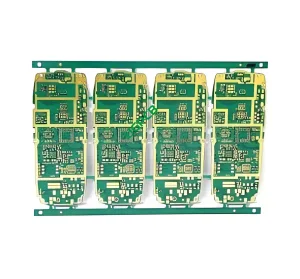
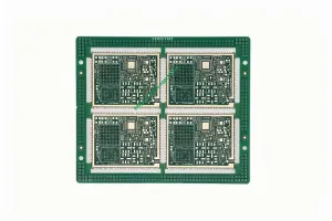
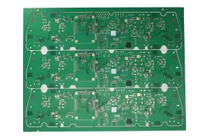
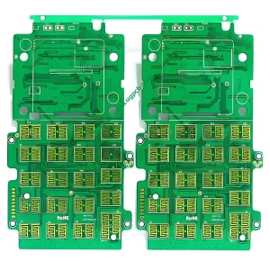
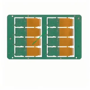
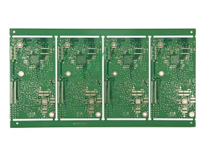
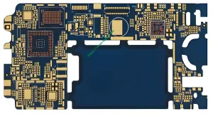
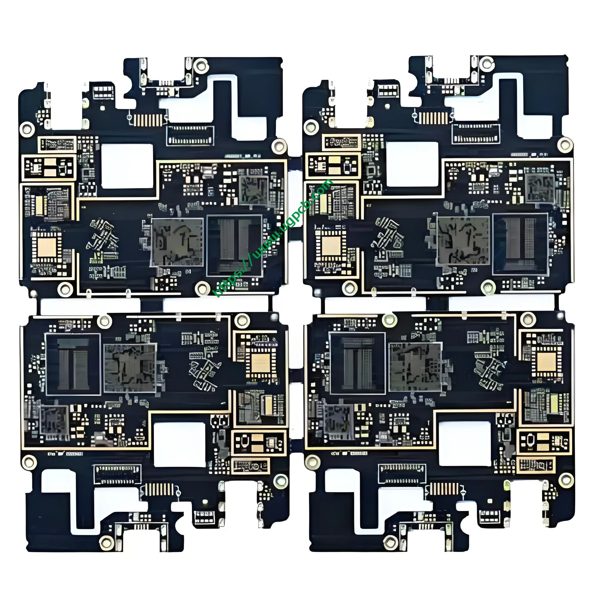
UGPCB แนะนำ 6‑layer 2+N+2 HDI PCB (แบบอย่าง: 6L 2+N+2 HDI PCB). This high‑density interconnect แผงวงจรพิมพ์ is engineered specifically for communication equipment. It uses ITEQ IT150 high‑performance laminate, combined with a second‑order HDI build‑up architecture, 2.5mil/2.5mil fine‑line trace and space, และ 0.1mm laser microvias. These features deliver reliable interconnections for 5G base stations, high‑speed network switches, โมดูลออปติคอล, และแอปพลิเคชันที่คล้ายกัน.
ใน พีซีบี อุตสาหกรรม, HDI (การเชื่อมต่อระหว่างกันที่มีความหนาแน่นสูง) technology is the core enabler for shrinking component pitches and rising signal speeds. ที่ 2+N+2 HDI PCB architecture represents the second‑order HDI category. It achieves an optimal balance among routing density, ความสมบูรณ์ของสัญญาณ, และต้นทุนการผลิต.
What Is a 2+N+2 HDI PCB?
Definition and Nomenclature
“2+N+2” is a standardized naming convention for HDI stack‑up structures. It is defined in theIPC-2226 standard and is classified asประเภทที่สาม within that system.
Breaking down the term:
- ที่ first “2” means two sequential build‑up layers above the core.
- “N” stands for the number of core layers (here N=2, เช่น., two inner core layers).
- ที่ second “2” means two sequential build‑up layers below the core.
ดังนั้น, a 2+N+2 structure adds two build‑up layers on each side of the conventional core. These are constructed throughtwo sequential lamination cycles. This 6‑layer board therefore comprises: 2 outer build‑up layers + 2 inner core layers + 2 outer build‑up layers.

การจำแนกประเภท HDI ตาม IPC‑2226
The IPC‑2226 standard defines several HDI types based on microvia structures and build‑up layer counts:
| ประเภท HDI | โครงสร้าง | Build‑up Layers (ต่อด้าน) | Minimum BGA Pitch | การใช้งานทั่วไป |
|---|---|---|---|---|
| ประเภทที่ 1 | 1+ยังไม่มี+1 | 1 ชั้น | 0.5มม | สมาร์ทโฟน, mid‑density designs |
| Type II/III | 2+ยังไม่มี+2 | 2 ชั้น | 0.4มม | อุปกรณ์เครือข่าย, high‑performance computing |
| ประเภทที่สาม / เอลิค | 3+N+3 and above | 3+ ชั้น | 0.3mm and below | สมาร์ทโฟนเรือธง, AI modules |
This product falls into the2+N+2 category. It features two build‑up layers per side, with microvias that can be arranged in eitherstacked or staggered การกำหนดค่า.
ข้อมูลจำเพาะทางเทคนิคหลัก
| พารามิเตอร์ | ข้อมูลจำเพาะ |
|---|---|
| แบบอย่าง | 6L 2+N+2 HDI PCB |
| วัสดุ | ITEQ IT150 |
| จำนวนเลเยอร์ | 6 ชั้น (2+N+2 second‑order HDI) |
| สีหน้ากากประสาน | สีดำหรือสีขาว (ไม่จำเป็น) |
| ความหนาของบอร์ดสำเร็จรูป | 1.0มม |
| ความหนาของทองแดงชั้นใน | 1 ออนซ์ (~35μm) |
| ความหนาของทองแดงชั้นนอก | 0.5 ออนซ์ (~17.5μm) |
| การติดตามขั้นต่ำ / ระยะห่าง | 2.5MIL / 2.5MIL (~63.5μm / ~63.5μm) |
| Minimum Mechanical Drill | 0.2มม |
| Minimum Laser Drill | 0.1มม |
| พื้นผิวเสร็จสิ้น | ทองแช่ + โอป |
| การสมัครหลัก | อุปกรณ์สื่อสาร |
Material Deep Dive: ITEQ IT150
Material Positioning
ITEQ IT150 คือ medium‑Tg, halogen‑free, multifunctional epoxy ลามิเนต. It sits between standard FR-4 and high‑performance low‑loss materials. It delivers lead‑free process compatibility, good manufacturability, and cost‑effectiveness.
The IT150GS variant (within the IT150 family) is a medium‑Tg (ทีจี >150°C โดย DSC), halogen‑free, middle‑loss material. It offers high thermal reliability and excellent CAF resistance. It is specifically designed for server, พื้นที่จัดเก็บ, and networking applications.
พารามิเตอร์ประสิทธิภาพหลัก
Based on ITEQ official datasheets and IPC‑TM‑650 test methods:
| คุณสมบัติ | วิธีทดสอบ | ค่าทั่วไป | หน่วย |
|---|---|---|---|
| อุณหภูมิการเปลี่ยนแก้ว (ทีจี) | DSC (IPC‑2.4.25) | 155 | องศาเซลเซียส |
| อุณหภูมิการสลายตัว (TD, 5% การสูญเสีย) | TGA (IPC‑2.4.24.6) | 365 | องศาเซลเซียส |
| CTE แกน Z (A1, ด้านล่าง Tg) | IPC‑2.4.24 | 35–40 | ppm/° C |
| CTE แกน Z (A2, เหนือ Tg) | IPC‑2.4.24 | 220–240 | ppm/° C |
| X/Y‑axis CTE (40–125°C) | IPC‑2.4.41 | 11/13 | ppm/° C |
| ค่าคงที่ไดอิเล็กตริก (ดีเค) @ 1GHz | IPC‑2.5.5.13 | 4.2–4.5 | - |
| ปัจจัยการกระจาย (ฟ) @ 1GHz | IPC‑2.5.5.13 | 0.010–0.018 | - |
| T288 Thermal Stress | IPC‑TM‑650 | >60 | Minutes |
| การดูดซับความชื้น | IPC‑2.6.2.1 | 0.12 | % |
| คะแนนความไวไฟ | UL94 | วี-0 | การให้คะแนน |
| UL MOT (Max Operating Temp) | - | 130 | องศาเซลเซียส |
ข้อดีของวัสดุ
1. Lead‑Free Process Compatibility
Standard FR‑4 typically has a Tg around 130°C. ITEQ IT150 delivers155องศาเซลเซียส. Under lead‑free reflow peaks of260องศาเซลเซียส, this higher Tg provides superior dimensional stability. The material resists excessive Z‑axis expansion, which significantly reduces the risk of via barrel cracking and pad lifting during assembly.
2. ต้านทาน CAF ได้ดีเยี่ยม
คาเฟ่ (เส้นใยขั้วบวกนำไฟฟ้า) is a primary failure mode in PCBs. It occurs when electrochemical migration creates short circuits under humid and hot conditions. ITEQ IT150 offershigh CAF resistance (18l / less than 100mil). This makes it especially suitable for long‑term outdoor deployment in communication infrastructure.
3. Halogen‑Free Compliance
ITEQ IT150 meetsJPCA‑ES‑01‑2003 halogen‑free standards. Chlorine (Cl) และโบรมีน (บ) content are each below 0.09% โดยน้ำหนัก. Total Cl+Br is below 0.15% (1500PPM).
แนวทางการออกแบบ
Stack‑Up Architecture
The 2+N+2 HDI PCB is manufactured throughsequential lamination:
- Core fabrication – Start with a double‑sided copper‑clad laminate. Etch inner layer circuits, perform mechanical drilling (0.2มม), and plate to create buried via connections.
- First build‑up – Apply prepreg and copper foil (or RCC) to both sides of the core. Execute the first lamination cycle.
- First laser drilling – Drill first‑order blind vias (laser holes at 0.1mm) and fill them with copper.
- Second build‑up – Apply additional dielectric layers and copper foil. Execute the second lamination cycle.
- Second laser drilling – Drill second‑order blind vias (0.1มม) and fill with copper.
- Outer layer circuits – Form outer layer circuits (trace/space 2.5mil) and apply the surface finish.
นี้two‑sequential‑lamination process is precisely what the “2” in 2+N+2 signifies.
Fine‑Line Circuit Design
ผลิตภัณฑ์นี้ประสบความสำเร็จ 2.5ล้าน/2.5ล้าน (~63.5μm/63.5μm) ความกว้างของการติดตามและระยะห่าง. This exceeds the เอชดีไอ ดีไซน์ Level C (60‑99μm) defined in IPC‑2226. This fine‑line capability enables:
- 0.4mm pitch BGA breakout with ample routing channels.
- Flexible signal routing for high‑density ส่วนประกอบ ตำแหน่ง.
- Reduced layer count, which lowers overall PCB cost.
เทคโนโลยี Microvia
ผลิตภัณฑ์นี้ใช้กhybrid drilling approach:
- การเจาะเครื่องกล – Minimum diameter 0.2มม, used for through‑holes and buried vias in the core.
- การขุดเจาะเลเซอร์ – Minimum diameter 0.1มม (4MIL) , used for blind vias in build‑up layers.
The 0.1mm laser microvia reduces via area by75% compared to a 0.2mm mechanical hole. This significantly frees up routing space. It is fundamental to achieving high‑density interconnect and enablingผ่านในแพด designs for fine‑pitch BGAs.
หลักการทำงาน
The 2+N+2 HDI PCB works through amulti‑layer interconnect architecture:
- Core‑layer interconnection – Buried vias, formed by การขุดเจาะเชิงกล + ชุบ, connect signals between core layers.
- Build‑up interconnection – Blind vias, formed by การเจาะด้วยเลเซอร์ + ชุบ, connect outer signal layers to inner layers.
- Full‑board through‑holes – After stack‑up completion, mechanical drilling penetrates all layers to create through‑holes.
- Signal transmission path – High‑speed signals travel from surface BGA pads → through laser blind vias into inner layers → across buried vias through the core → through laser blind vias on the opposite side to the bottom layer.
นี้stepped interconnect structure shortens signal paths and reduces parasitic via effects. เป็นผลให้, it preserves high‑speed signal integrity.
ข้อดีด้านประสิทธิภาพ
ความน่าเชื่อถือทางความร้อน
ITEQ IT150’sTD (decomposition temperature) reaches 365°C, which is well above the lead‑free reflow peak of 260°C. T288 thermal stress testingexceeds 60 นาที without delamination. This ensures material integrity through multiple reflow cycles.
ความสมบูรณ์ของสัญญาณ
ที่ 1GHz, ITEQ IT150 exhibits a dielectric constant Dk of approximately 4.2–4.5 and a dissipation factor Df of 0.010–0.018. As a “standard‑to‑mid‑loss” material, IT150 provides a compelling price‑performance ratio compared to ultra‑low‑loss materials. This makes it ideal for production‑ready communication equipment.
ความแข็งแรงเชิงกล
ITEQ IT150 deliversflexural strength of 470–500 N/mm² in the warp direction and 400–430 N/mm² in the fill direction. This ensures structural integrity throughout assembly and field deployment.
การจำแนกประเภทผลิตภัณฑ์
This product is classified across multiple dimensions:
| Classification System | หมวดหมู่ |
|---|---|
| IPC‑2226 HDI Type | Type II/III (2+ยังไม่มี+2, double build‑up per side) |
| HDI Order | Second‑order (2 laser drilling cycles + 2 lamination cycles) |
| Rigid/Flexible | PCB แข็ง |
| จำนวนเลเยอร์ | 6‐บอร์ดหลายชั้น |
| ระบบวัสดุ | Medium‑Tg, halogen‑free, FR‑4‑compatible epoxy |
| พื้นผิวเสร็จสิ้น | ทองแช่ + OSP hybrid finish |
| โดเมนแอปพลิเคชัน | Communication‑grade PCB |
ผังกระบวนการผลิต
UGPCB follows this production sequence for the 6‑layer 2+N+2 HDI PCB:
ขั้นตอน 1: Core Layer Fabrication
Material cutting → Inner layer dry film → Etching → AOI inspection → Brown oxide treatment
ขั้นตอน 2: First Build‑Up
การเคลือบ (แกนกลาง + เตรียมการ + ฟอยล์ทองแดง) → First lamination → First‑order laser drilling (0.1มม) → Desmear → Electroless copper + plating → Circuit patterning
ขั้นตอน 3: Second Build‑Up
Second lamination → Second lamination → Second‑order laser drilling (0.1มม) → Desmear → Electroless copper + plating → Circuit patterning
ขั้นตอน 4: Outer Layer and Finishing
การเจาะเครื่องกล (0.2mm through‑holes) → Electroless copper + plating → Outer layer circuits (2.5ล้าน/2.5ล้าน) → Solder mask → Immersion Gold + OSP surface finish → Electrical testing → Final inspection → Packaging and shipment
The entire process involvestwo lamination cycles and two laser drilling operations. This demands exceptional process control and precision.

สถานการณ์การใช้งาน
This product is primarily designed forอุปกรณ์สื่อสาร:
5โครงสร้างพื้นฐานการสื่อสาร
- 5สถานีฐาน G (gNB) – RF front‑end and baseband processing units.
- High‑speed backplane interconnects for 5G network equipment.
- Enterprise‑grade routers and core switches.
High‑Speed Data Transmission
- 400G/800G optical modules – control and signal processing boards.
- High‑speed fiber‑optic switches.
- เครื่องรับส่งสัญญาณแสง.
Other High‑End Applications
- High‑performance servers and storage devices.
- AI inference/training accelerator cards.
- Advanced medical imaging equipment.
The 2+N+2 HDI structure is particularly well‑suited formoderate pin‑count, high‑density BGA การกำหนดเส้นทาง. It enables complex signal interconnects within limited board space.
ทำไมต้องเลือก UGPCB?
UGPCB brings deep manufacturing expertise to HDI PCB production:
- Fine‑line capability – 2.5mil/2.5mil trace/space in volume production, meeting advanced HDI design requirements.
- Mature microvia process – 0.1mm laser via + 0.2mm mechanical drill hybrid solution with stable yield.
- Comprehensive material certification – Full qualification on ITEQ IT150 and other mainstream material systems.
- End‑to‑end process control – Every step from cutting to electrical testing strictly follows ไอพีซี-6012 rigid PCB qualification and performance specifications.
- Communication industry track record – Extensive experience in 5G base station, optical module, and network equipment การผลิต PCB.
ขอใบเสนอราคาวันนี้เลย
Whether you are designing high‑speed backplanes for 5G base stations or developing next‑generation optical modules, UGPCB’s 6‑layer 2+N+2 HDI PCB provides the reliable interconnect foundation your project deserves.
การประกาศแหล่งข้อมูล
The technical data cited in this document comes from the following authoritative standards and sources:
- IPC-2226 - Sectional Design Standard for High Density Interconnect (HDI) บอร์ดพิมพ์
- IPC‑6012E/F - ข้อกำหนดคุณสมบัติและประสิทธิภาพสำหรับบอร์ดพิมพ์แข็ง
- IPC/JPCA‑2315 - Design Guide for High Density Interconnect Structures and Microvias
- ITEQ IT‑150 / IT‑150GS Official Datasheets and Material Specifications
- IPC‑TM‑650 – Test Methods Manual (including methods 2.4.4, 2.4.24, 2.4.24.6, 2.4.25, 2.5.5.13, 2.6.2.1, และอื่น ๆ)
- JPCA‑ES‑01‑2003 - Halogen‑Free Copper‑Clad Laminate Standard
- UL94 - มาตรฐานความปลอดภัยความไวไฟของวัสดุพลาสติกสำหรับชิ้นส่วนในอุปกรณ์และเครื่องใช้