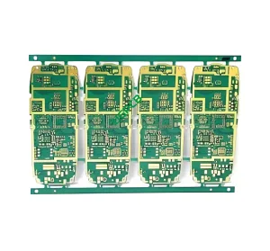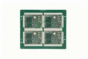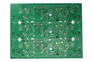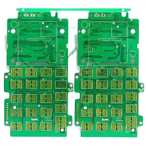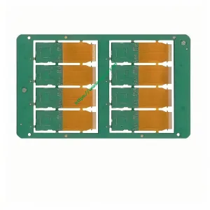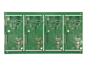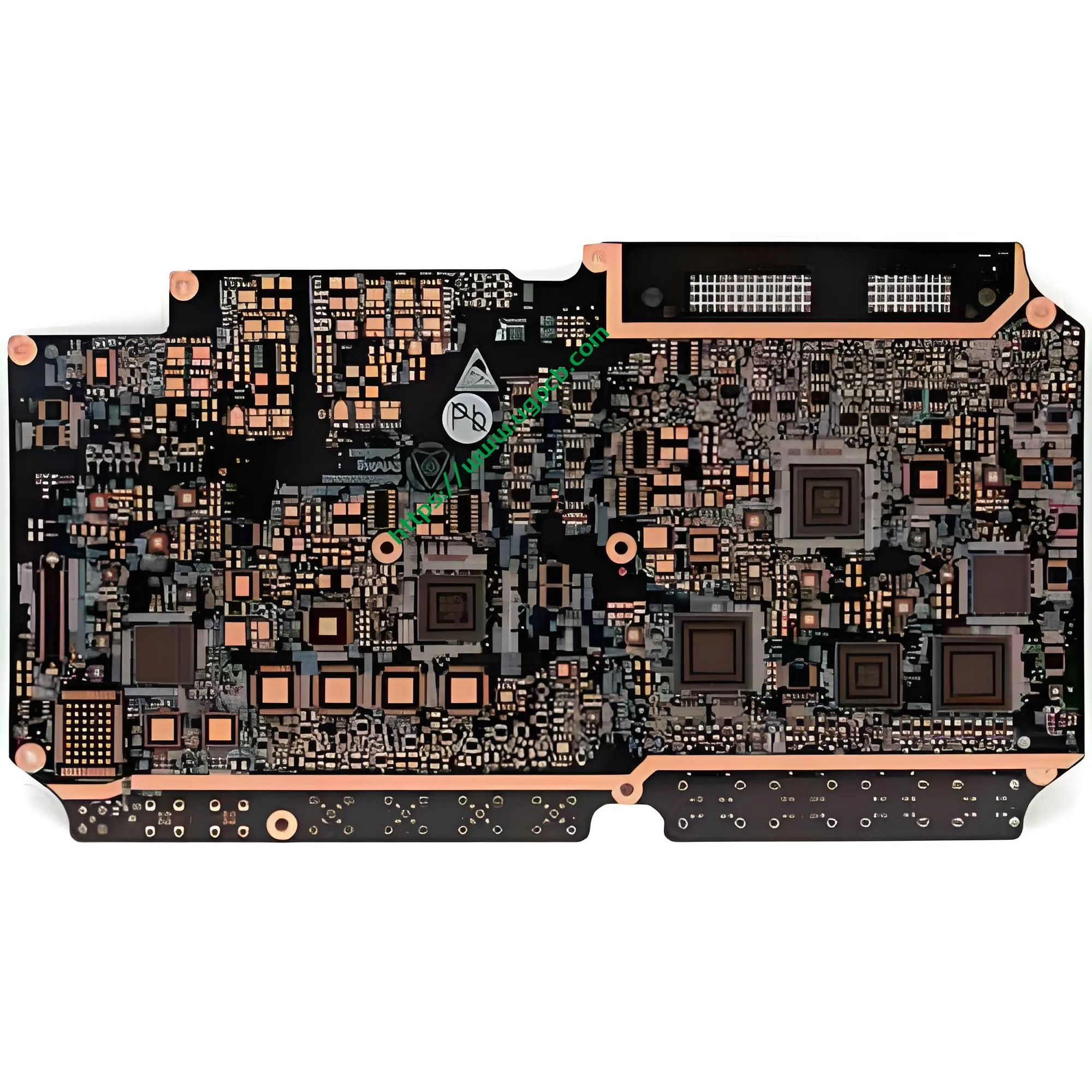
1. ภาพรวมผลิตภัณฑ์: What Is an Automotive Communication 2+N+2 HDI Board?
ที่Automotive Communication 2+N+2 HDI Board คือ การเชื่อมต่อระหว่างกันที่มีความหนาแน่นสูง (HDI) แผงวงจรพิมพ์ engineered specifically for vehicle communication systems. This product adopts a14-ชั้น stack-up structure withS1000-2M high-performance copper-clad laminate as the core substrate material. It achieves high-density, high-reliability interlayer interconnection through an advanced process combining2 laser drilling cycles และ3 lamination cycles.
Within the เอชดีไอ พีซีบี classification system, 2+ยังไม่มี+2 denotes a specific build-up structure—adding 2 build-up layers on each side of the core substrate (N layer) using the sequential build-up (SBU) วิธี. Compared to 1+N+1 (first-order HDI), 2+N+2 represents asecond-order HDI สารละลาย, offering higher wiring density and more sophisticated interconnection capabilities.
UGPCB, as a professional ผู้ผลิต PCB, delivers high-quality เอชดีไอ พีซีบี products that comply with the IPC-6012FA automotive applications addendum—the industry’s most stringent reliability standard for automotive electronics.

2. การจำแนกประเภทผลิตภัณฑ์: Scientific Positioning and Technology Tier
This product can be scientifically classified across multiple dimensions:
By IPC-6012 Performance Class: Class 3/A—the highest reliability tier for automotive electronics. IPC-6012F tightens through-hole resistance change after thermal cycling from 10% ถึงกmaximum of 5% for Class 3/A, and increases minimum barrel copper thickness from 25 อืมถึง28 ไมโครเมตร.
By HDI Order: Second-Order HDI (2+ยังไม่มี+2)—a mid-complexity HDI solution positioned between first-order HDI (common in consumer electronics) and high-end any-layer HDI.
By Material Loss Tier: Mid-Loss (ฟ < 0.010).
ตามโดเมนแอปพลิเคชัน: Automotive Electronics—in-vehicle communication, อดาส, V2X, ฯลฯ.
ตามระดับความไวไฟ: อล 94 วี-0—the highest vertical burn rating, requiring self-extinguishment within 10 seconds with no flaming drips.
3. Core Parameters and Technical Specifications
| พารามิเตอร์ | ข้อมูลจำเพาะ | มาตรฐานอ้างอิง |
|---|---|---|
| ลามิเนต | เอส1000-2เอ็ม (เซิงยี่เทคโนโลยี) | IPC-4101/126 |
| จำนวนเลเยอร์ | 14 เลเยอร์ | - |
| ความหนาของบอร์ด | 1.6 ± 0.16 มม | ไอพีซี-6012F |
| Minimum Laser Via Diameter | 0.10 มม | - |
| Minimum Mechanical Hole Diameter | 0.20 มม | - |
| ความกว้างการติดตามขั้นต่ำ / ระยะห่าง | 75 ไมโครเมตร / 75 ไมโครเมตร | ไอพีซี-2221C |
| อัตราส่วนภาพ | 8:1 | ไอพีซี-2221 |
| อุณหภูมิการเปลี่ยนแก้ว (ทีจี) | 180องศาเซลเซียส (DSC) | IPC-TM-650 2.4.25 |
| อุณหภูมิการสลายตัวทางความร้อน (TD) | 355องศาเซลเซียส | Shengyi S1000-2M Datasheet |
| ค่าคงที่ไดอิเล็กตริก (Dk @ 1GHz) | 4.6 | Shengyi S1000-2M Datasheet |
| ปัจจัยการกระจาย (Df @ 1GHz) | 0.013 | Shengyi S1000-2M Datasheet |
| คะแนนความไวไฟ | อล 94 วี-0 | อล 94 มาตรฐาน |
| กระบวนการพิเศษ | 2 การขุดเจาะเลเซอร์, 3 Laminations | - |
Aspect Ratio Calculation is a critical process parameter in การผลิต PCB that directly determines plating quality and through-hole reliability. ตามแนวทาง IPC-2221, Aspect Ratio = Board Thickness ÷ Drilled Hole Diameter. For this product: 1.6 mm ÷ 0.2 มม. = 8:1. IPC-2221 recommends a maximum aspect ratio of 8:1 ถึง 10:1 for conventional electrolytic plating processes. ที่ 8:1 design ensures reliability while fully validating UGPCB’s process capability in high-aspect-ratio through-hole plating.
4. Material Deep Dive: S1000-2M High-Performance Substrate
S1000-2M is a high-performance FR-4.0 copper-clad laminate manufactured by Shengyi Technology. มันคือกlead-free compatible high-Tg material.
พารามิเตอร์ประสิทธิภาพหลัก (แหล่งที่มา: Shengyi Technology official datasheet and IPC-TM-650 test methods):
| พารามิเตอร์ | ค่า | วิธีทดสอบ |
|---|---|---|
| ทีจี (อุณหภูมิการเปลี่ยนแก้ว) | 180องศาเซลเซียส (DSC) | IPC-TM-650 2.4.25 |
| TD (อุณหภูมิการสลายตัวทางความร้อน) | 355องศาเซลเซียส | Shengyi Datasheet |
| T260 | > 60 นาที | IPC-TM-650 |
| T288 | 30 นาที | IPC-TM-650 |
| ซีทีอี (แกน Z, ด้านล่าง Tg) | 41 ppm/° C | IPC-TM-650 |
| ซีทีอี (แกน Z, เหนือ Tg) | 208 ppm/° C | IPC-TM-650 |
| ความแข็งแรงของเปลือก (after 288°C solder float) | 1.3 n/mm | IPC-TM-650 |
Core Advantages of S1000-2M:
- Mid-Loss Characteristics: With a Df of 0.013 @ 1GHz, this material offers approximately28% lower dielectric loss compared to standard FR-4 (Df ≈ 0.018).
- ต้านทานความร้อนสูง: Tg of 180°C and Td of 355°C meet the stringent requirement of continuous operation above 125°C in automotive environments.
- คาเฟ่ (เส้นใยขั้วบวกนำไฟฟ้า) ความต้านทาน: Suitable for high-multilayer PCBs and high-humidity environments.
- อล 94 วี-0 คะแนนความไวไฟ: Self-extinguishes within 10 seconds with no flaming drips.
5. สิ่งจำเป็นสำหรับการออกแบบ: 2+N+2 HDI Architecture Explained
5.1 What Is the 2+N+2 Structure?
The 2+N+2 HDI board is manufactured using the sequential build-up method:
- N Layer: The core substrate layer (multilayer core formed by inner-layer lamination)
- 2 Build-up Layers on Each Side: Constructed sequentially through 2 laser drilling cycles and 2 lamination cycles on both sides of the core
2 Laser Drilling Cycles respectively form the microvias for the first build-up layer (L1-L2, L13-L14) and the second build-up layer (L2-L3, L12-L13).
3 Lamination Cycles รวม: core layer lamination → first build-up layer lamination → second build-up layer lamination.
5.2 เทคโนโลยี Microvia
- Laser Blind Vias: 0.10 mm diameter, formed using CO₂ or UV laser drilling
- Mechanical Buried Vias: 0.20 mm diameter, used for interlayer interconnection within the core
- Stacked/Staggered Via Design: Supports stacked or staggered microvia structures for maximum layout flexibility
5.3 Fine-Line Circuitry
Minimum trace width and spacing of 75 ไมโครเมตร (ประมาณ 3 MIL) comply with IPC-2221C requirements for fine-line design. This precision supports fan-out routing for 0.5 mm pitch BGAs.
5.4 การควบคุมความต้านทาน
With a Dk of 4.6 @ 1GHz, S1000-2M enables characteristic impedance control at 50Ω, 90โอ้, and 100Ω through adjustment of trace width and dielectric thickness—meeting the signal integrity requirements of in-vehicle communication systems.
6. หลักการทำงาน: How Does an HDI Board Achieve High-Density Interconnection?
Traditional multilayer PCBs rely onทะลุผ่านรู that penetrate the entire board thickness for layer-to-layer connections—consuming significant routing area.เอชดีไอ พีซีบี technology overcomes this limitation through several innovations:
1. คนตาบอดผ่านเทคโนโลยี: Laser-drilled microvias connect only the outer layer to the adjacent inner layer (เช่น, L1-L2) โดยไม่ต้องเจาะทั้งกระดาน.
2. Buried Via Technology: Mechanically drilled vias are completely contained within the core layer (เช่น, L3-L12) and do not appear on the board surface.
3. Sequential Build-Up Method: Build-up layers are constructed sequentially, with each additional layer providing additional routing resources.
4. Stacked Via Interconnection: Blind vias on upper and lower layers can be stacked in alignment to create signal paths spanning multiple layers.
In a 14-layer 2+N+2 structure, a signal can travel from the surface layer (L1) through a 0.10 mm laser blind via to L2, then through a second-layer laser blind via to L3, then through a mechanical buried via within the core to L12, and finally through symmetrical build-up blind vias to the bottom layer (L14)—achievingsignal transmission across 14 layers without consuming surface-layer routing area.
7. ลักษณะประสิทธิภาพ: Why Is This Board Ideal for Automotive Communication?
7.1 IPC-6012FA Automotive Standard Compliance
ในเดือนธันวาคม 2025, IPC (now the Global Electronics Association) officially releasedIPC-6012FA, ที่Automotive Applications Addendum to IPC-6012F Qualification and Performance Specification for Rigid Printed Boards. This addendum applies to rigid printed boards that must survive the vibration and thermal cycling environments of electronic interconnects within the automotive industry.
ไอพีซี-6012F (released October 2023) represents the most significant tightening of automotive PCB reliability requirements in over a decade. Key changes include:
- Through-Hole Resistance Change: Tightened from 10% ถึงกmaximum of 5% for Class 3/A
- Barrel Copper Thickness: Increased from 25 อืมถึง28 ไมโครเมตร for Class 3/A
- IST (Interconnect Stress Testing): Changed from optional tomandatory, ขั้นต่ำของ500 รอบ for Class 3/A
- Stacked Microvias: Requiringseparate qualification at the stacked via level
7.2 Thermal Cycling Reliability
Automotive electronics face continuous operating temperaturesabove 125°C in engine compartments and EV battery-adjacent environments. With Tg of 180°C, Td of 355°C, T260 > 60 นาที, and T288 of 30 นาที, S1000-2M ensures dimensional stability and dielectric performance under extreme thermal conditions.
7.3 ความสมบูรณ์ของสัญญาณ
In-vehicle communication systems (V2X, อดาส, Automotive Ethernet) continue to push operating frequencies higher. With a Df of 0.013 @ 1GHz, S1000-2M is a mid-loss material that supports10G–25G SerDes channels with excellent performance over link lengths up to 20 นิ้ว.
7.4 Vibration Resistance
IPC-6012FA specifically addresses automotive vibration environments. The 14-layer HDI board’s multilayer laminated structure provides excellent mechanical strength. การรวมกันของ 0.10 mm laser microvias and 0.20 mm mechanical holes ensures connection reliability under vibration.
8. กระบวนการผลิต: จากวัตถุดิบสู่ผลิตภัณฑ์สำเร็จรูป
ขั้นตอน 1: Inner-Layer Core Fabrication
- Core material cutting → inner-layer circuit imaging → etching → AOI inspection
ขั้นตอน 2: First Lamination
- Stack multiple inner-layer cores with prepreg → high-temperature high-pressure lamination → core substrate (N layer) การก่อตัว
ขั้นตอน 3: First Laser Drilling & การชุบ
- First laser drilling on both sides of the core (forming L1-L2, L13-L14 microvias) → desmear → electroless copper deposition → electrolytic copper filling
ขั้นตอน 4: First Build-Up Lamination
- Laminate first build-up layer material on both sides of the core →Second Lamination
ขั้นตอน 5: Second Laser Drilling & การชุบ
- Second laser drilling (forming L2-L3, L12-L13 microvias) → desmear → electroless copper deposition → electrolytic copper filling
ขั้นตอน 6: Second Build-Up Lamination
- Laminate second build-up layer material on both sides of the core →Third Lamination
ขั้นตอน 7: การขุดเจาะเครื่องกล
- Drill 0.20 mm mechanical through-holes and buried vias (within L3-L12 core)
ขั้นตอน 8: Outer-Layer Circuit Fabrication
- Outer-layer circuit imaging → etching → solder mask → surface finish (เห็นด้วย, ฯลฯ)
ขั้นตอน 9: การตรวจสอบขั้นสุดท้าย
- Electrical testing → โพรบบิน testing → final AOI → reliability sampling (IST, การปั่นจักรยานด้วยความร้อน, ฯลฯ)
9. สถานการณ์การใช้งาน: Core Interconnection Solutions for In-Vehicle Communication Systems
1. ระบบช่วยเหลือผู้ขับขี่ขั้นสูง (อดาส)
ADAS requires multi-sensor fusion (เรดาร์คลื่นมิลลิเมตร, ลิดาร์, กล้อง). The 2+N+2 HDI board supports microstrip antenna integration and RF impedance control in radar modules with its high-density interconnection capability.

2. V2X (Vehicle-to-Everything) การสื่อสาร
V2X modules demand integration of communication RF front-ends, การประมวลผลเบสแบนด์, and power management within compact spaces—making HDI PCB’s high-density characteristics an ideal choice.
3. Automotive Ethernet
10G/25G automotive Ethernet switches require stringent signal integrity control. S1000-2M’s mid-loss characteristics ensure low-loss transmission for high-speed signals.
4. Zonal Controllers
Next-generation vehicle architecture zonal controllers process massive data volumes. The 14-layer 2+N+2 HDI board provides ample routing layers and flexible interconnection structures.
5. ระบบการจัดการแบตเตอรี่ (BMS)
EV battery management system PCBs must maintain long-term reliability in high-temperature, high-vibration environments—exactly the scenario addressed by S1000-2M material and IPC-6012FA standards.
10. ทำไมต้องเลือก UGPCB?
- IPC-6012FA Compliance: Strict adherence to the latest automotive PCB standard released December 2025
- Advanced HDI Manufacturing Capability: Supporting 2+N+2, 3+N+3, and any-layer HDI structures
- วัสดุที่ผ่านการรับรอง: S1000-2M certified to UL 94 วี-0, compliant with IPC-4101/126 specifications
- การควบคุมคุณภาพแบบครบวงจร: Full-process inspection from raw materials to finished products, ensuring Class 3/A reliability
- การตอบสนองอย่างรวดเร็ว: Professional engineering team providing DFM (ออกแบบเพื่อการผลิต) ความคิดเห็น
📞 Request a Quote Today
UGPCB specializes in the R&D and manufacturing ofautomotive electronics HDI PCBs. ไม่ว่าคุณจะต้องการ2+N+2 HDI boards, 14-layer high-multilayer PCBs, or otherautomotive communication PCB การแก้ปัญหา, we provide one-stop services from design optimization to volume production.
📧 Send your Gerber files or technical requirements to: sales@ugpcb.com
🔗 Visit the UGPCB website for an instant quote
การประกาศแหล่งข้อมูล
ข้อมูลทางเทคนิคและข้อมูลมาตรฐานที่อ้างถึงในเอกสารนี้มาจากแหล่งข้อมูลที่เชื่อถือได้ดังต่อไปนี้:
- IPC (Global Electronics Association) — ไอพีซี-6012Fข้อกำหนดคุณสมบัติและประสิทธิภาพสำหรับบอร์ดพิมพ์แข็ง (ตุลาคม 2023), IPC-6012FAAutomotive Applications Addendum (December 2025), ไอพีซี-2221Cมาตรฐานทั่วไปเกี่ยวกับการออกแบบแผ่นพิมพ์ (สิงหาคม 2025), IPC-4101Eข้อกำหนดสำหรับวัสดุฐานสำหรับบอร์ดพิมพ์แข็งและหลายชั้น, IPC-TM-650คู่มือวิธีทดสอบ
- เซิงยี่เทคโนโลยี — S1000-2M Product Datasheet and Technical Data Sheet
- อล (ห้องปฏิบัติการรับประกันการจัดจำหน่าย) — ยูล 94 วี-0 Flammability Rating Standard
บันทึก: All data is cited from publicly available official standard documents or manufacturer specifications to the greatest extent possible. Specific values may vary slightly due to test conditions and batch differences. Readers are advised to refer to the latest official documentation for the most current specifications.