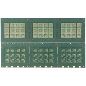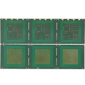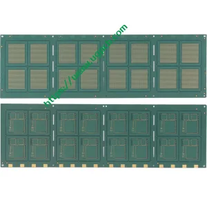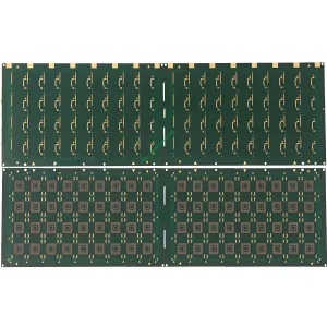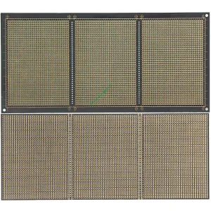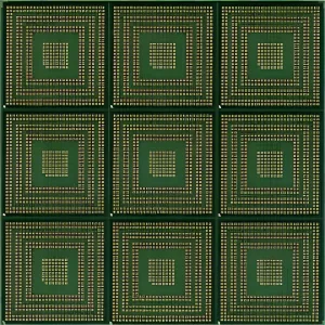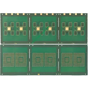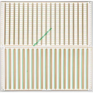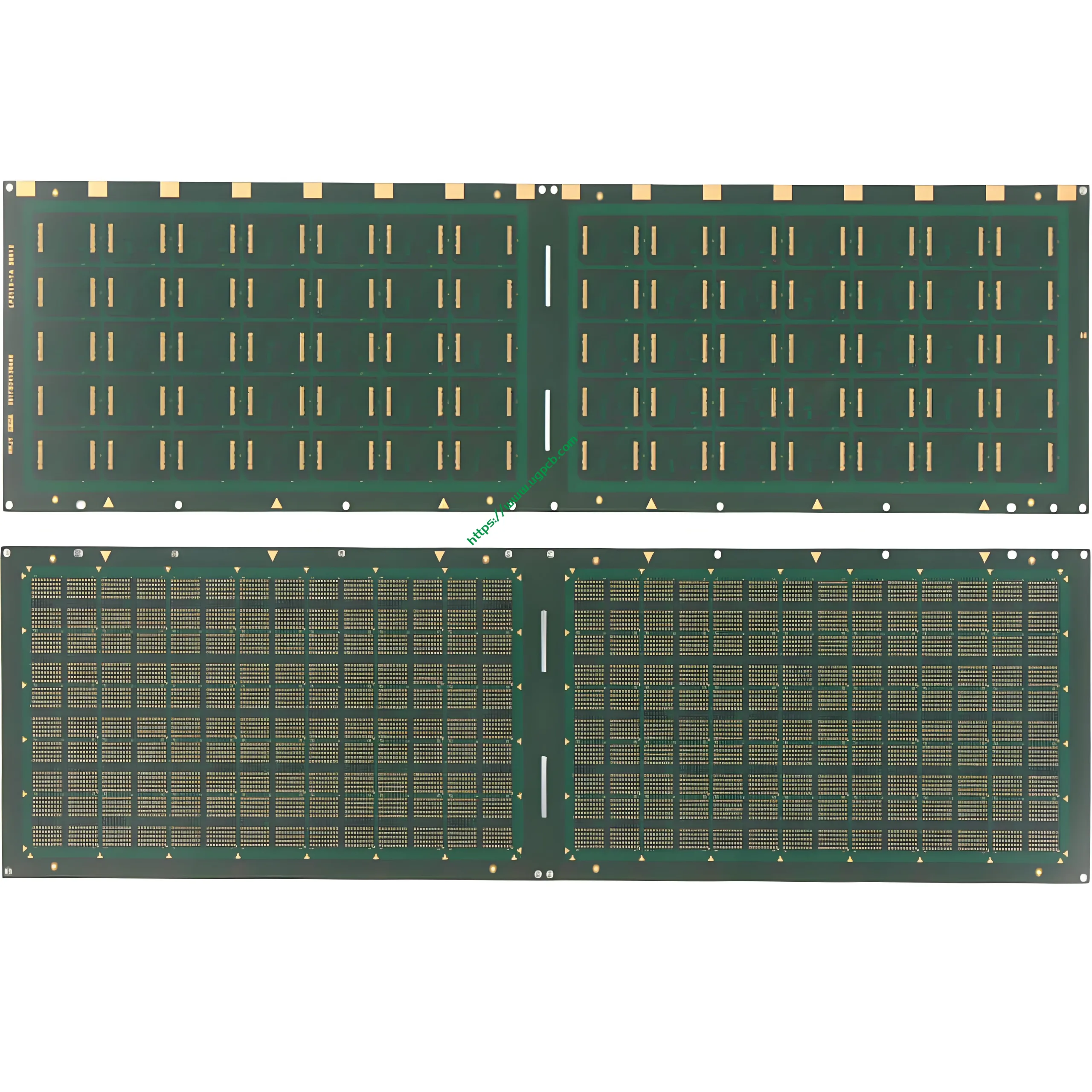
Lead the High-Speed Era: UGPCB’s 4-Layer DDR Substrate Board – The Superior Interconnect Solution for Your Core ICs
In the booming landscape of high-performance computing, ปัญญาประดิษฐ์, and next-generation communication devices, every advancement in Double Data Rate (ดีดีอาร์) technology places stricter demands on PCB substrates. โดยอาศัยความเชี่ยวชาญเชิงลึกในด้าน high-end PCB manufacturing และ สารตั้งต้น IC การแก้ปัญหา, UGPCB introduces its premium 4-Layer DDR Substrate Board. Engineered with cutting-edge materials, it is specifically designed to carry high-performance memory chips (เช่น, DDR4, DDR5, LPDDR), serving as your reliable partner in the pursuit of ultimate speed and stability.
ภาพรวมผลิตภัณฑ์ & คำนิยาม
อัน 4-Layer DDR Substrate Board is a High-Density Interconnect (HDI) printed circuit board designed for packaging and connecting Dynamic Random-Access Memory (ดีดีอาร์) ชิป. It acts as a critical bridge between the chip and the mainboard, responsible for transmitting high-speed signals, distributing power, and providing stable mechanical support. ไม่เหมือนมาตรฐาน บอร์ด PCB, DDR substrates demand near-perfect signal integrity, การจัดการความร้อน, and dimensional accuracy. This product from UGPCB is tailor-made to meet these stringent requirements.
ข้อควรพิจารณาการออกแบบที่สำคัญ
-
การควบคุมความต้านทานที่แม่นยำ: Paramount for DDR PCB design, it minimizes signal reflection and distortion during high-speed data transmission.
-
ความสมบูรณ์ของพลังงาน (PI): Dedicated power and ground plane design ensures clean, stable power delivery, reducing noise interference on critical signals.
-
ความสมบูรณ์ของสัญญาณ (และ): Optimized routing using microstrip and stripline structures minimizes crosstalk and delay, forming the foundation for stable performance post-แอสเซมบลี PCBA.
-
-
การจัดการความร้อน: The substrate material must exhibit excellent thermal properties to aid chip dissipation and ensure long-term reliability.
มันทำงานอย่างไร
The 4-Layer DDR Substrate connects the hundreds of micro-pins of a memory chip to the corresponding motherboard circuits via its precise internal layers. ของมัน “แซนด์วิช” กองขึ้น (สัญญาณ-กราวด์-พลังงาน-สัญญาณ) provides clear return paths for high-speed signals, effectively suppressing Electromagnetic Interference (อีเอ็มไอ). The soft gold surface finish ensures a reliable, low-resistance solder joint with the chip’s solder balls (เช่น, in BGA packages).
แอปพลิเคชันหลัก & การจำแนกประเภท
-
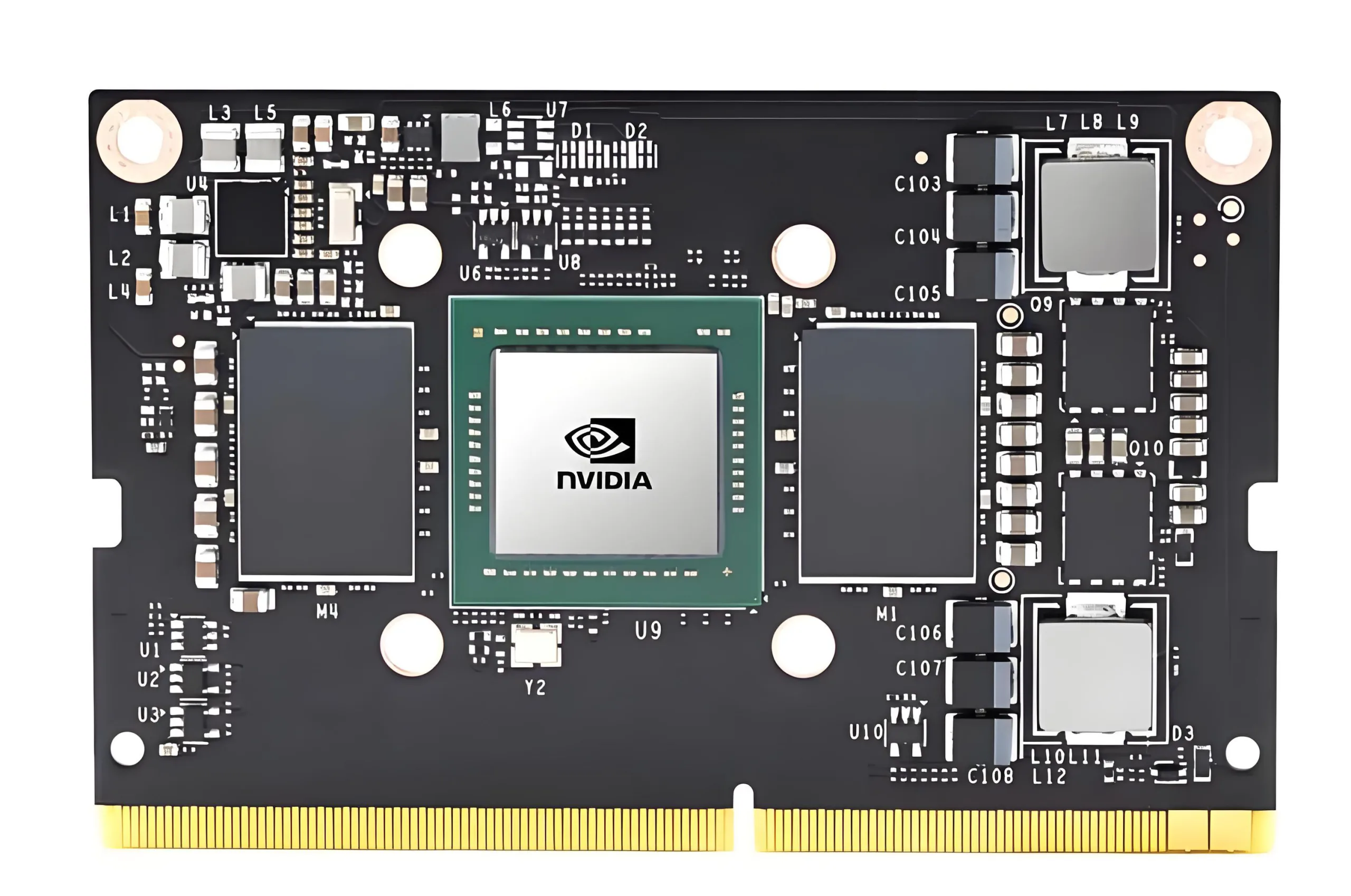
แอปพลิเคชันหลัก: Extensively used in servers, สวิตช์ศูนย์ข้อมูล, high-end GPUs, การ์ดเร่งความเร็ว AI, network storage devices, and any cutting-edge electronic product requiring high-speed, high-capacity memory.
-
การจำแนกประเภท:
-
โดยการนับเลเยอร์: Beyond standard 4-layer, designs can extend to 6, 8, or more layers based on complexity.
-
โดยวัสดุ: Can be categorized into standard FR-4, Mid-Loss, and this product’s focus – Low-Loss material substrates.
-
วัสดุ & ข้อมูลจำเพาะด้านประสิทธิภาพ
| พารามิเตอร์ | ข้อมูลจำเพาะ | ข้อได้เปรียบด้านประสิทธิภาพ |
|---|---|---|
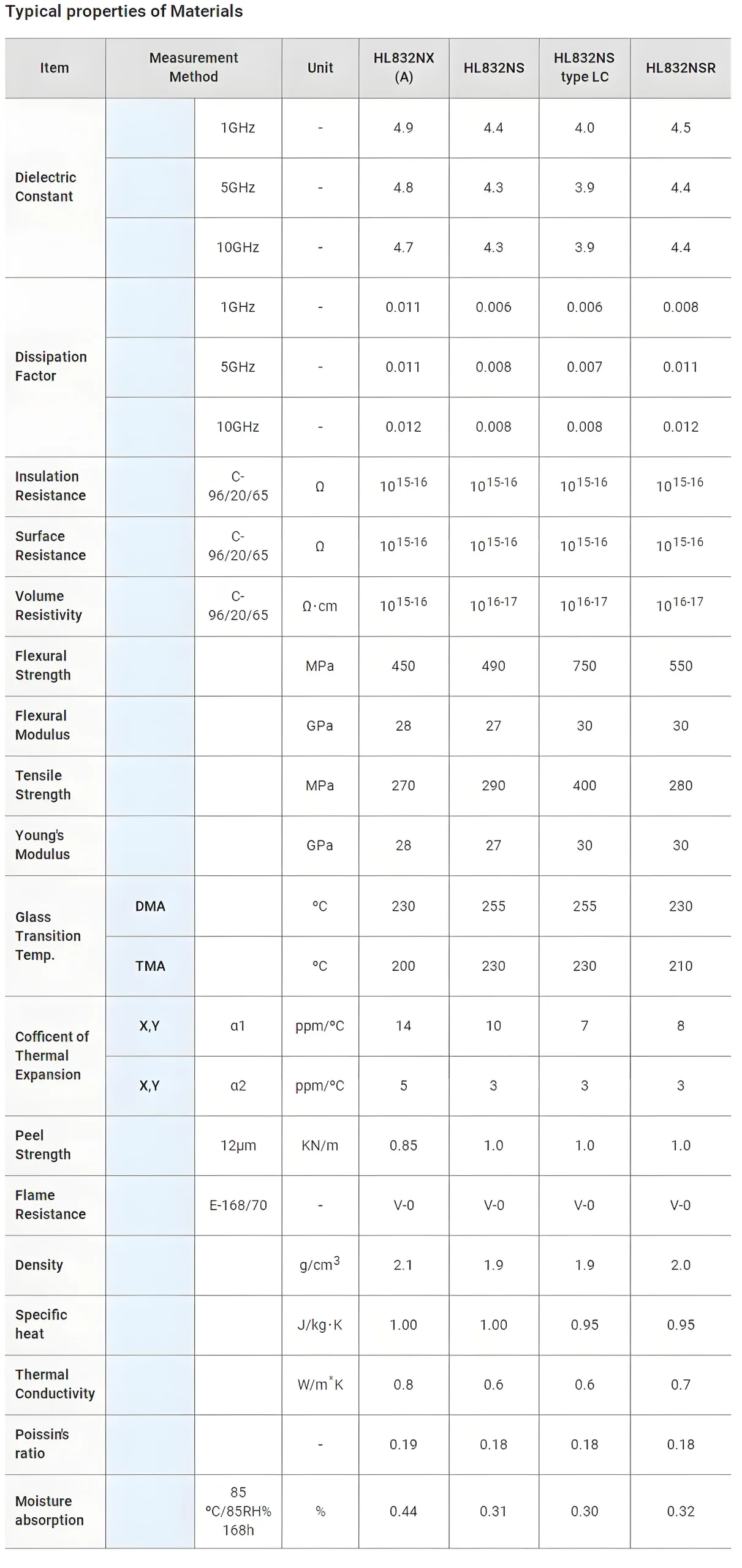
| วัสดุหลัก | Mitsubishi Gas Chemical HL832 | Industry-recognized, ประสิทธิภาพสูง, low-loss (Low Df) laminate designed for high-speed digital circuits, significantly reducing signal transmission loss. |
| จำนวนเลเยอร์ | 4 เลเยอร์ | Optimal “สัญญาณ-กราวด์-พลังงาน-สัญญาณ” กองขึ้น, balancing design complexity, ค่าใช้จ่าย, และประสิทธิภาพ. |
| ความหนาสำเร็จรูป | 0.25มม | Ultra-thin profile, conforming to compact chip packaging trends for integration into miniaturized devices. |
| ความหนาของทองแดง | 0.5ออนซ์ (17.5μm) | Standard starting weight, suitable for fine-line etching; can be plated up for higher current needs. |
| สีหน้ากากประสาน | สีเขียว (AUS308) | Provides excellent insulation protection and visual contrast for Optical Inspection (Aoi) หลังจาก การประกอบ PCB. |
| พื้นผิวเสร็จสิ้น | ทองอ่อน (เห็นด้วย) | Excellent surface planarity and low hardness, ensures superior compatibility with wire bonding or BGA solder balls for reliable connections. |
| Minimum Drilled Hole Size | 100μm | Supports high-density micro-via design for complex chip pinout interconnection. |
| นาที. ความกว้างของเส้น/ช่องว่าง | 50μm / 75μm | High-precision routing capability allows more high-speed lines in limited space, การประชุม high-density interconnect PCB design needs. |
โครงสร้างผลิตภัณฑ์ & คุณสมบัติที่สำคัญ
-
โครงสร้าง: Typical 4-layer sequential lamination: ชั้นบนสุด (Signal/Components) -> ชั้นใน 1 (Solid Ground Plane) -> ชั้นใน 2 (Solid Power Plane) -> ชั้นล่าง (Signal/Components). This structure offers optimal shielding for high-speed signals.
-
คุณสมบัติที่สำคัญ:
-
Superior High-Speed Performance: HL832 low-loss material ensures excellent signal integrity for high-frequency DDR signals.
-
ความสามารถในการเชื่อมต่อระหว่างกันที่มีความหนาแน่นสูง: 100μm micro-vias and 50μm line width technology support advanced chip packaging.
-
ความน่าเชื่อถือสูง: ENIG surface finish offers excellent solderability and oxidation resistance for long-term stability.
-
บางเฉียบ & แม่นยำ: 0.25mm overall thickness meets stringent space requirements in modern electronics.
-
 กระบวนการผลิตที่แม่นยำ
ของเรา การผลิต PCB process adheres to the highest quality standards:
Material Prep → Inner Layer Imaging & Etching → Lamination & Drilling → Metallization & Plating → Outer Layer Imaging → Surface Finish (เห็นด้วย) → Solder Mask Application → Profiling → Electrical Test & การตรวจสอบขั้นสุดท้าย.
Each stage is supported by advanced inspection equipment (เช่น, Aoi, การทดสอบโพรบบิน), ensuring every สารตั้งต้น IC delivered is flawless.
กรณีการใช้งานทั่วไป
This 4-Layer DDR Substrate is the ideal choice for:
-
ศูนย์ข้อมูล & เซิร์ฟเวอร์: Carrying CPU and memory modules for massive data processing.
-
AI & Machine Learning Hardware: Memory subsystems in GPU, NPU accelerator cards.
-
อุปกรณ์สื่อสารระดับไฮเอนด์: High-speed memory units in 5G base stations and core network gear.
-
เครื่องใช้ไฟฟ้าชั้นนำ: Main memory substrates in top-tier gaming consoles and laptops.
Why Choose UGPCB’s 4-Layer DDR Substrate?
We are more than a ผู้ผลิต PCB; we are your solution provider for high-speed design challenges. With a dedicated รองรับการออกแบบ PCB team, proven capabilities in multilayer PCB prototyping and mass production, and a deep understanding of signal integrity engineering, choosing UGPCB means gaining not just a high-quality substrate, but an accelerator for your product’s success.
Contact our expert team today for a project-specific quote and technical consultation. Power up your high-speed design with UGPCB!