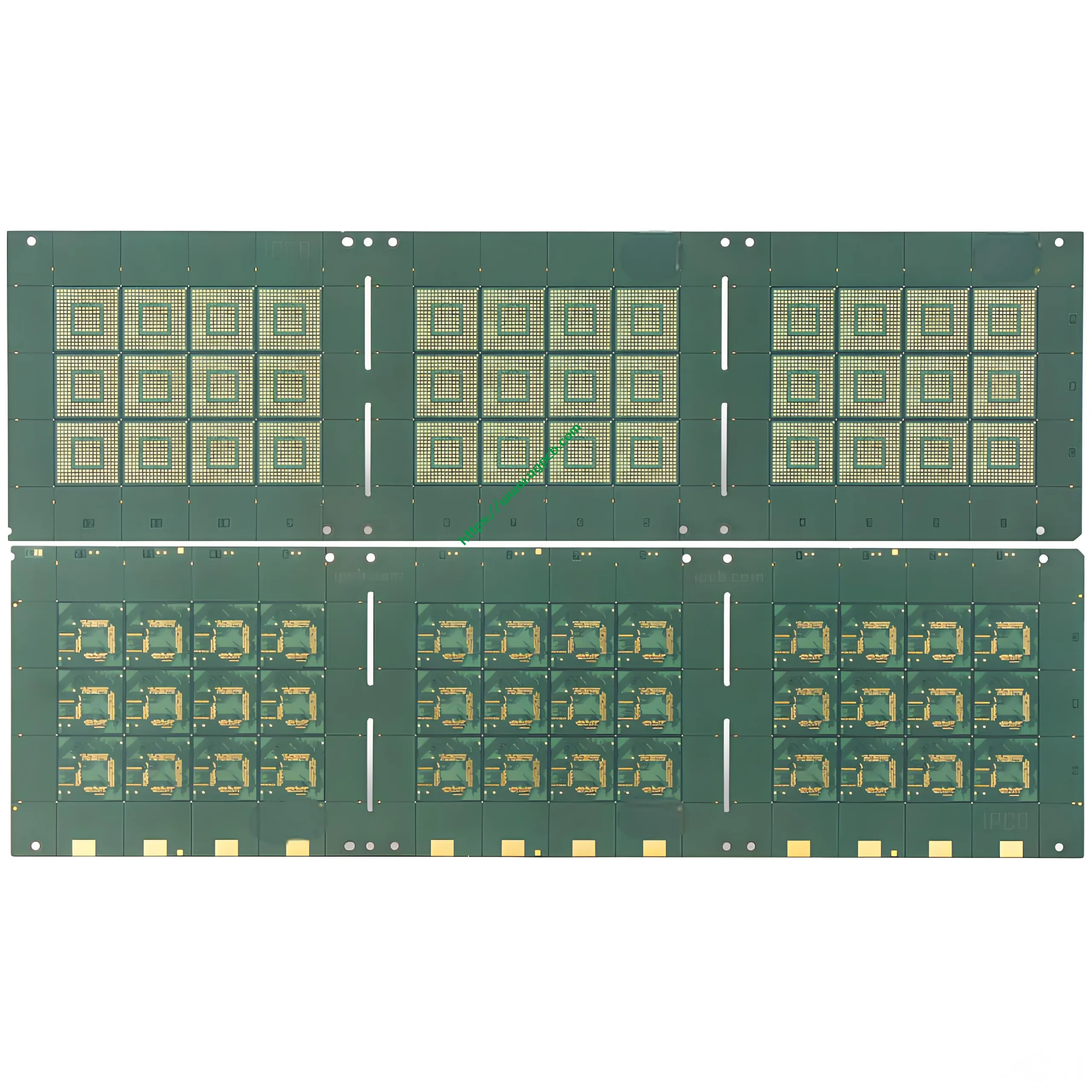
High-Performance BGA IC Substrate: The Precision Foundation for Advanced IC Packaging
In the era of smaller, เร็วขึ้น, and more powerful electronics, advanced IC packaging is critical. Acting as the essential interface between the silicon die and the main แผงวงจรพิมพ์ (พีซีบี), ที่ พื้นผิว BGA IC is the core component of high-end semiconductor packages. UGPCB leverages deep การผลิต PCB expertise and advanced processes to deliver high-performance, เชื่อถือได้ BGA package substrate การแก้ปัญหา.
1. What is a BGA IC Substrate?
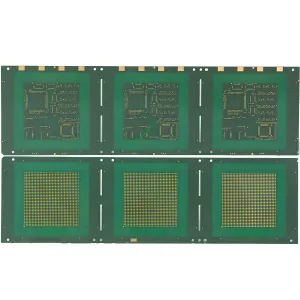
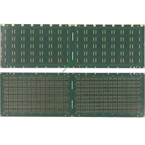
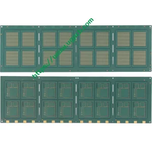
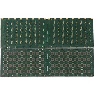
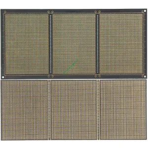
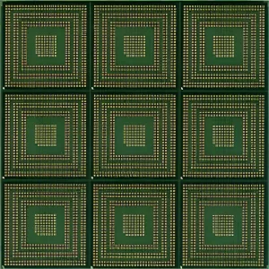
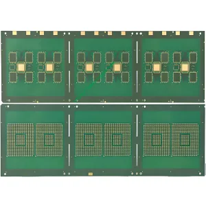
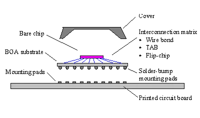
A BGA IC Substrate is a specialized type of การเชื่อมต่อระหว่างกันที่มีความหนาแน่นสูง (HDI) พีซีบี designed explicitly for Ball Grid Array (BGA) การบรรจุหีบห่อ. It is not a standard แผงวงจร but a precision multilayer interconnect structure. One side interfaces with the die via ultra-fine circuitry, while the opposite side connects to the main บอร์ด PCB through an array of solder balls, fulfilling four key functions: การเชื่อมต่อโครงข่ายไฟฟ้า, การส่งสัญญาณ, การกระจายความร้อน, and physical support.
2. สิ่งจำเป็นสำหรับการออกแบบ & หลักการปฏิบัติงาน
สิ่งจำเป็นสำหรับการออกแบบ:
-
Ultra-High Wiring Density: To accommodate increasing I/O counts, substrates require ultra-fine line design. UGPCB reliably achieves 30μm/30μm minimum line width/space, enabling efficient fan-out routing for high-pin-count chips.
-
Precise Registration & ความเสถียรของมิติ: Alignment between die and solder balls must be extremely accurate. Our core material, มิตซู แก๊ส HF BT HL832NX-A-HS, offers a low CTE (ค่าสัมประสิทธิ์การขยายตัวทางความร้อน) และความเสถียรของมิติที่ดีเยี่ยม, preventing warpage and misalignment caused by thermal stress.
-
Reliable Microvias: Layer-to-layer interconnection depends on laser-drilled blind vias. ของเรา 0.075การเจาะด้วยเลเซอร์ มม capability facilitates high-density vertical connections (เช่น, 1-2, 3-4 ชั้น), รับประกันความสมบูรณ์ของสัญญาณ.
-
Optimized Signal & ความสมบูรณ์ของพลังงาน: A carefully designed stack-up (เช่น, 1L-4L, 1L-2L, 3L-4L as per your specs) and plane allocation provide low-loss paths for high-speed signals and clean, stable power delivery to the chip.
หลักการปฏิบัติงาน:
The die is attached to the substrate’s top surface (typically Layer 1) via wire bonding or flip-chip technology. Electrical signals from the chip are routed, redistributed (อาร์ดีแอล), and transmitted through the substrate’s internal ultra-fine traces และ microvias (laser/mechanical holes). They finally exit via the solder ball array on the bottom surface to connect to the larger พีซีบี (การประกอบ PCB). It is essentially a miniaturized, chip-specific, high-end แผงวงจรพิมพ์.
3. วัสดุหลัก, โครงสร้าง & คุณสมบัติที่สำคัญ
-
วัสดุหลัก: มิตซู แก๊ส HF BT HL832NX-A-HS high-performance laminate. Renowned for its ค่าคงที่ไดอิเล็กตริกต่ำ (ดีเค), low dissipation factor (ฟ), ต้านทานความร้อนสูง (ค่า Tg สูง), and exceptional dimensional stability, it is the ideal choice for high-speed, high-frequency IC packaging substrates.
-
Key Structure: 4-layer build with stacked via design (1-2, 3-4 จุดแวะตาบอดชั้น) for greater routing density. The overall PCB thickness is 0.3mm, meeting thin-profile packaging requirements.
-
พื้นผิวเสร็จสิ้น:****เกี่ยวกับ enepic (อิเล็กโทรไลต์นิกเกิลอิเล็กโทรไลเซิลแพลเลเดียม, 2ม.”). This finish combines nickel’s barrier properties, palladium’s corrosion resistance, and gold’s superior solderability. It is the preferred choice for fine-pitch BGA solder ball สิ่งที่แนบมา, สร้างความมั่นใจในระยะยาว.
-
หน้ากากบัดกรี & Opening: เราใช้ ไทโย PSR4000 AUS308 high-performance Liquid Photoimageable Solder Mask (LPSM), known for high resolution and reliability, perfectly defining openings for 0.1mm mechanical through-holes and pads.
4. การจำแนกประเภท & แอปพลิเคชันหลัก
-
การจำแนกประเภท: Primarily categorized by interconnection method: Wire Bonding Substrates และ Flip Chip Substrates. The specifications provided (ultra-fine lines, เกี่ยวกับ enepic) are particularly suited for Flip Chip and other advanced packaging applications.
-
แอปพลิเคชันหลัก:
-
หน่วยประมวลผลกลาง (CPU/GPU) การบรรจุหีบห่อ
-
Mobile Device Application Processors (AP) & Baseband Chips
-
High-Speed Networking & Communication Chips (เช่น, เอฟพีจีเอ, เอสิค)
-
ปัญญาประดิษฐ์ (AI) & Machine Learning Accelerators
-
Advanced Memory Packaging (เช่น, HBM)
-
These applications represent the core of ความหนาแน่นสูง, high-performance PCBA ออกแบบ.
-
5. UGPCB’s BGA IC Substrate Production Process & การควบคุมคุณภาพ
ของเรา BGA circuit board manufacturing ปฏิบัติตามอย่างเข้มงวด, high-standard flow:
Inner Layer Imaging → Laser Drilling / Mechanical Drilling → Hole Metallization (การชุบทองแดง) → Outer Layer Imaging → Solder Mask Application (PSR4000) → ENEPIG Surface Finish → Electrical Testing → Final Inspection.
The entire process occurs in controlled cleanroom environments (Class 10K/1K), utilizing Automated Optical Inspection (Aoi), laser measurement systems, และอีกมาก, ensuring every BGA packaging PCB meets chip-level reliability standards.
6. Why Choose UGPCB for Your BGA IC Substrate?
-
Premium Material Assurance: Core laminates from top-tier suppliers like Mitsubishi Gas guarantee performance from the start.
-
ความสามารถของกระบวนการขั้นสูง: 30/30μm line/space and 0.075mm laser microvias support the most cutting-edge chip packaging designs.
-
Ultra-Thin Core Expertise: Proven experience in high-yield, volume production of 0.3mm and thinner boards.
-
Comprehensive Surface Finish Options: We offer various high-end finishes including ENEPIG to meet different bonding/soldering needs.
-
One-Stop Service: จาก ทบทวนการออกแบบ PCB และ ต้นแบบแบบหมุนเร็ว ไปจนถึงปริมาณการผลิต, we provide end-to-end PCBA substrate solutions for your new chip project.
บทสรุป:
As we approach the physical limits of Moore’s Law, advanced packaging is key to continued electronics performance growth. Choosing a reliable พื้นผิว BGA IC lays a solid foundation for your chip’s success. Whether you are involved in chip design, การบรรจุหีบห่อ, การทดสอบ, หรือ การผลิต PCBA, UGPCB เป็นพันธมิตรที่เชื่อถือได้ของคุณ.
ติดต่อเราวันนี้ to discuss your BGA package substrate, เอชดีไอ พีซีบี ความต้องการ, and request a quote. Let’s collaborate to enable the next generation of electronic innovation!