
UGPCB: High-Density Blind Vias IC Substrate for Advanced Semiconductor Packaging
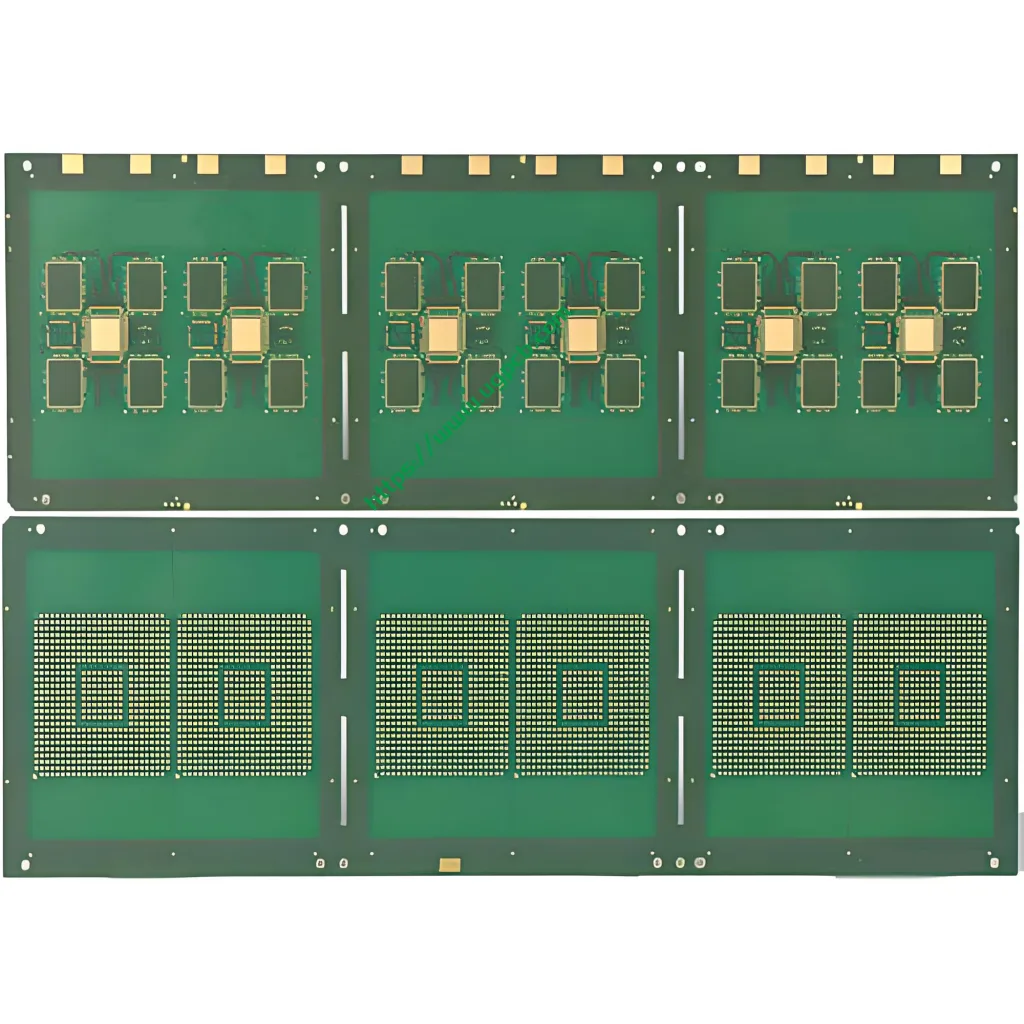
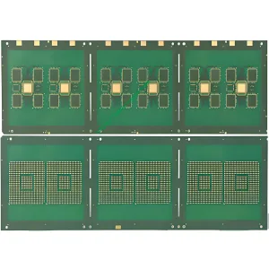
UGPCB’s 8-layer Blind Vias IC Substrate, built with Mitsubishi Gas HF HL832NX material, enables superior signal integrity and high-density interconnects for next-generation chips, featuring 30μm line width and 0.1mm micro vias.
As electronics rapidly evolve toward การย่อขนาดเล็ก, higher density, and enhanced performance, traditional through-hole via technology struggles to meet the demands of modern chip packaging. Blind Via technology has emerged as a critical solution for การเชื่อมต่อระหว่างกันที่มีความหนาแน่นสูง (HDI) ออกแบบ.
A Blind Via is a conductive hole that connects an outer layer of a PCB to one or more inner layers without passing through the entire board. UGPCB’s 8-Layer Blind Vias IC Substrate, utilizing Mitsubishi Gas HF material, exemplifies this advanced technology, providing a precision, reliable interconnection platform for advanced semiconductor packaging.
Core Product: In-Depth Look at Blind Vias IC Substrates
Blind Via technology defines a specific type of interconnect structure that connects an outer layer to an adjacent inner layer only. Unlike a through-hole via, a blind via starts on the board surface and terminates precisely at a specific inner copper layer.
This structure maximizes usable wiring space by eliminating unnecessary through-board holes, significantly increasing circuit density—a perfect match for the industry’s drive toward smaller form factors and greater integration.
From a technical implementation perspective, the design and fabrication of blind vias adhere to strict standards, such as those outlined in the ไอพีซี-6012 qualification and performance specification for rigid PCBS. They are typically formed using laser drilling processes, creating a tapered hole structure. This allows for precise control over depth and diameter, meeting the stringent requirements of advanced packaging for micro-features and registration accuracy.
ข้อกำหนดทางเทคนิค & Design Advantages
The design of UGPCB’s Blind Vias IC Substrate is highly specialized, involving critical considerations from material selection to stack-up architecture.
Key Technical Parameters:
-
แบบอย่าง: พื้นผิว IC Vias ตาบอด
-
Core Material: Mitsubishi Gas HF (HL832NX) BT Epoxy
-
จำนวนเลเยอร์: 8 เลเยอร์
-
ความหนาโดยรวม: 0.6 มม
-
Board Dimensions: 40 mm x 55 มม
-
หน้ากากบัดกรี: PSR-4000 AUS308
-
พื้นผิวเสร็จสิ้น: Soft (Electroless Nickel Immersion) ทอง
-
Minimum Laser Drilled Via Diameter: 0.1 มม
-
Minimum Line Width / ช่องว่าง: 30 μm / 30 μm
This substrate employs Japan’s Mitsubishi Gas Chemical HF series BT material (HL832NX), known for excellent dielectric properties (ดค/ดฟ) และ เสถียรภาพทางความร้อน, making it ideal for high-frequency and high-speed applications. ที่ 30μm fine line technology is critical for connecting high-pin-count chips, while the ENIG surface finish provides a flat, wire-bondable, and reliable soldering surface.
มันทำงานอย่างไร: Precision Interconnection & ความสมบูรณ์ของสัญญาณ
The core function of a Blind Vias IC Substrate is to establish efficient, reliable interlayer electrical connections while minimizing real estate consumption—directly addressing modern packaging needs for high density and superior performance.
For signal transmission, blind vias offer distinct advantages over through-hole vias. Through-holes can create unwanted stubs that act as antennae, degrading signal integrity at high frequencies. Vias ตาบอด, connecting only necessary layers, eliminate these non-functional stubs, reducing parasitic capacitance and inductance for cleaner, more stable signal paths.
The fabrication typically uses controlled-depth laser drilling, offering superior precision and consistency for micro-vias compared to mechanical drilling. This is crucial for maintaining high yield and quality in volume production.
Regarding signal integrity, the 30μm line/space design, combined with the optimized dielectric material, allows for precise การควบคุมความต้านทาน, minimizing reflection and loss—a paramount concern for RF and high-speed digital applications.
Types and Classification of Blind Via Structures
Blind via substrates can be categorized based on design architecture and application:
-
By Structure: Standard Blind Vias (connecting two adjacent layers) และ Stacked Blind Vias (multiple vias aligned vertically across several layers, used for complex, deep interconnects).
-
By Location: Blind Vias (from surface to inner layer) และ Buried Vias (connecting inner layers only, not exposed on either surface). The combination of these types enables highly complex interconnect routing.
Key Advantages and Differentiating Features
| คุณสมบัติ | Benefit | ผลกระทบ |
|---|---|---|
| ประสิทธิภาพพื้นที่ | Maximizes usable wiring area on inner layers. | Enables further miniaturization or increased functionality. |
| Enhanced Electrical Performance | Reduces signal stub effects and parasitics. | Improves signal integrity and speed for high-frequency chips. |
| Design Flexibility | Enables complex, high-density interlayer routing. | Facilitates advanced packaging like 2.5D/3D integration. |
| Improved Reliability | Reduces potential points for inner-layer short circuits. | Increases product longevity and field performance. |
กระบวนการผลิต: A Journey of Precision
The production of a Blind Vias IC Substrate is a precise and multi-step process:
-
ออกแบบ & Drilling File Generation: Using CAD tools (เช่น, Cadence, Mentor) following IPC-2581 แนวทางปฏิบัติ. Drill files specify via locations, sizes, and depths.
-
การเตรียมวัสดุ: Laminating copper foil onto the Mitsubishi HF core material.
-
การขุดเจาะเลเซอร์: Using CO₂ or UV lasers to ablate the dielectric and form the micro-vias with precise depth control.
-
Desmearing & การทำให้เป็นโลหะ: Plasma desmearing cleans the via hole, followed by electroless copper deposition to make the hole walls conductive.
-
Pattern Plating & Imaging: Applying photoresist, exposing, developing, and electroplating to build up circuit traces and via barrels.
-
การเคลือบ & การจัดตำแหน่งเลเยอร์: Bonding multiple etched layers with เตรียมการ (B-stage) dielectric under heat and pressure. Registration accuracy เป็นสิ่งสำคัญ (<±25 μm).
-
Final Processing: Applying solder mask (พีเอสอาร์-4000), พื้นผิวเสร็จสิ้น (เห็นด้วย), and electrical testing.
Primary Applications and Use Cases
Blind Vias IC Substrates are essential in demanding applications:
-
Advanced Consumer Electronics: สมาร์ทโฟน, แท็บเล็ต, and wearables utilize them for compact motherboard design, connecting application processors, หน่วยความจำ, and sensors.
-
อุปกรณ์อิเล็กทรอนิกส์ยานยนต์: Critical for ADAS radar modules, ระบบสาระบันเทิง, and engine control units (กล่อง ECU), where reliability under high temperature and vibration is key (aligned with IPC-6012DA for automotive).
-
โทรคมนาคม: 5G/6G base stations, network switches, and RF modules rely on them for excellent high-frequency signal integrity and impedance control.
-
High-Performance Computing (HPC): เซิร์ฟเวอร์, AI/ML accelerators, and GPUs use these substrates for dense, high-speed interconnects between silicon dies and memory.
Partner with UGPCB for your most challenging chip packaging projects. Our expertise in advanced materials like Mitsubishi HF and precision processes such as 30μm line technology and laser-drilled blind vias ensures your designs achieve optimal performance and reliability. Contact our engineering team today for a design review or prototype quote.


