
In the realms of semiconductor packaging and high-end electronics manufacturing, as chip functionalities grow increasingly complex and product sizes shrink, ที่ substrate that carries and interconnects delicate chips has become central to determining product performance and reliability. ที่ ส่วนประกอบพื้นผิว PCB จาก UGPCB is engineered precisely for this challenge. Utilizing advanced Substrate-Like พีซีบี (เอสแอลพี) processes and top-tier materials, it is specifically designed for advanced packaging and miniaturized components that demand ultra-high wiring density, exceptional signal integrity, and utmost reliability.
ภาพรวมผลิตภัณฑ์: คำนิยาม & Core Value Proposition
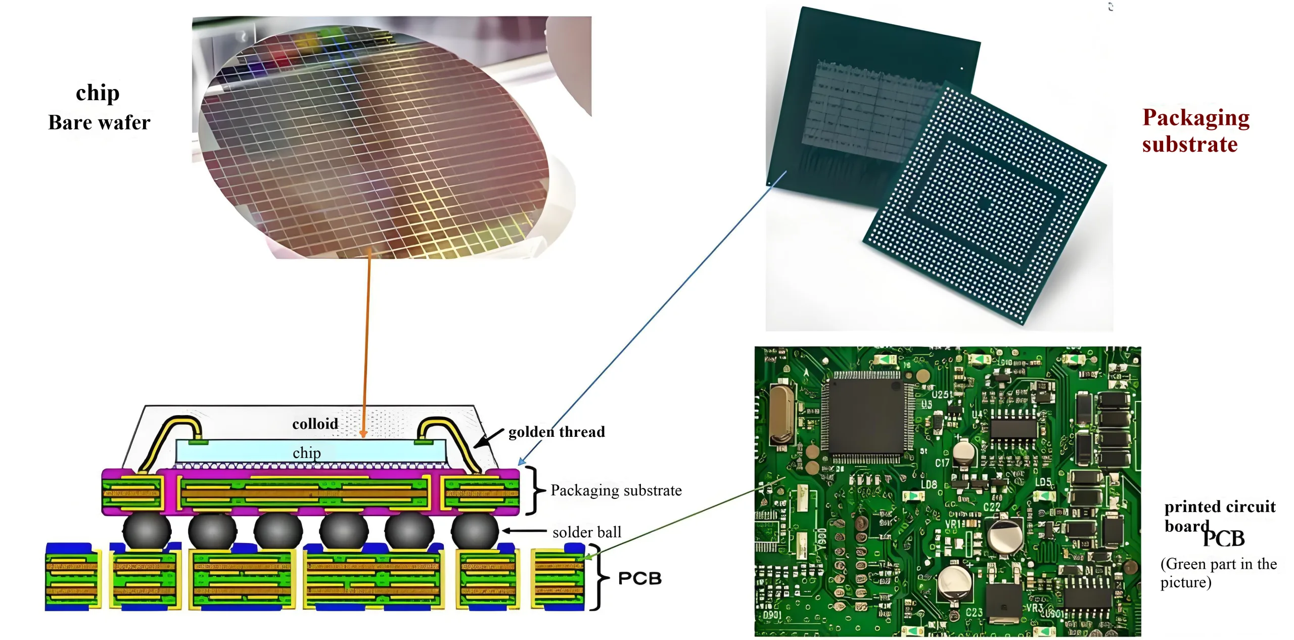
A Component Substrate PCB is a specialized type of แผงวงจรพิมพ์ that acts primarily as the critical interconnection bridge between a semiconductor chip and the main motherboard. Unlike standard PCBs, its design rules are closer to those of พื้นผิว IC used in semiconductor packaging but find broader application in carrying various active and passive ส่วนประกอบอิเล็กทรอนิกส์ to form a complete functional sub-module.
Think of it as the “micro-skeleton” และ “เครือข่ายประสาท” of an electronic device. After a wafer is diced into individual chips, they are first precisely packaged onto such a substrate before being assembled onto a larger main PCB. ดังนั้น, the substrate’s performance directly dictates the ultimate effectiveness of the chip it carries. UGPCB’s product targets the urgent need for miniaturization and high functional integration in premium consumer electronics, AI hardware, and advanced communication equipment.
Detailed Technical Specifications
This component substrate from UGPCB represents a high level of precision manufacturing, with its core specifications as follows:
-
จำนวนเลเยอร์ & โครงสร้าง: 2-layer design, providing precise double-sided interconnection within an ultra-thin profile for a compact structure.
-
ความหนาของบอร์ด: 0.3มม overall thickness, saving crucial internal space for ultra-slim device designs.
-
Line Fineness: การสนับสนุน minimum line width/space of 75 ไมโครมิเตอร์ (μm), enabling high-density routing in a minimal area, which is fundamental for complex functionalities.
-
Conductive Via Capability: คุณสมบัติ minimum drill hole size of 0.25mm, ensuring reliable, high-density electrical connections between layers.
-
พื้นผิวเสร็จสิ้น: Utilizes Hard Gold ชุบ. The gold layer offers excellent wear resistance, oxidation resistance, and can withstand repeated insertions and harsh environments, guaranteeing long-term contact reliability—ideal for connectors and critical test points.
-
หน้ากากบัดกรี & วัสดุ: Employs high-performance PSR-4000 WT03 solder mask ink for superior insulation and heat resistance. The core material is CC-HL820WDI, known for its exceptional dimensional stability and low Coefficient of Thermal Expansion (ซีทีอี). This effectively reduces stress caused by temperature fluctuations during soldering and operation, preventing circuit breakage or connection failure with the chip.
ข้อควรพิจารณาในการออกแบบ & หลักการทำงาน
Critical Design Focus
Designing a Component Substrate PCB requires thinking beyond conventional PCB rules, focusing on:
-
Signal Integrity First: The ultra-fine 75μm lines necessitate strict impedance control. Design must thoroughly account for the impact of skin effect and crosstalk on high-speed signals.
-
Co-Design for Thermal Management: As the primary seat for the chip, the substrate is a key heat dissipation path. It requires using high-thermal-conductivity materials and intelligent design of thermal vias and copper planes to efficiently draw heat away from the chip.
-
Mechanical Stress Compatibility: A core challenge is matching the differing CTE between the silicon chip and the substrate. The low CTE characteristic of CC-HL820WDI material is key to minimizing solder joint fatigue failure due to thermal cycling, thereby enhancing product lifespan in demanding environments.
มันทำงานอย่างไร: A Brief Explanation
The fundamental operating principle of a component substrate is to provide the semiconductor chip with a three-dimensional platform for electrical interconnection, physical support, and thermal management.
-
Electrical Connection: Through its internal precision copper traces and micro-vias, มัน “translates” และ “reroutes” the hundreds or even thousands of micron-scale pads on a chip into larger, more manageable footprints for easy soldering and routing on the main PCB.
-
การสนับสนุนทางกายภาพ: Provides a robust mechanical platform for the fragile silicon die, protecting it from physical damage.
-
Environmental Protection: Protects the internal fine-line circuitry from moisture, ฝุ่น, and chemical corrosion through the solder mask and potential underfill.
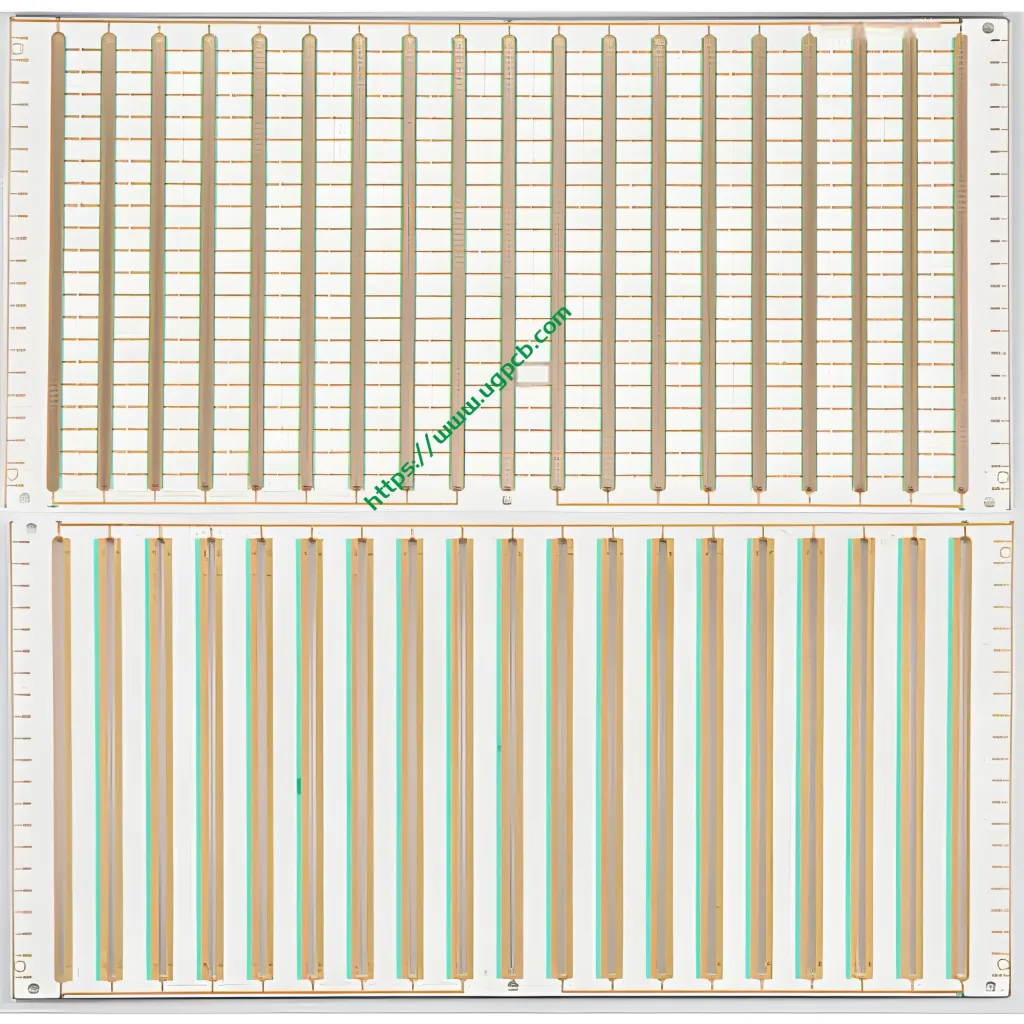
An illustration showing the microscopic structure of a Component Substrate PCB, highlighting its fine lines, micro-vias, and layered build-up.
Image Alt Text: Close-up cross-section diagram of a UGPCB Component Substrate PCB showing high-density traces and microvias
แอปพลิเคชันหลัก & การจำแนกประเภท
Key Application Areas
This high-precision component substrate is the unsung hero in many high-end electronic products:
-
Advanced Semiconductor Packaging: Widely used in เอฟซี-ซีเอสพี, จิบ (ระบบในแพ็คเกจ) and other advanced packaging formats as the primary chip carrier.
-
Miniaturized Modules: It is the key enabler for integrating full functionality into tiny spaces within micro sensor modules, mmWave antenna modules, and high-end camera modules.
-
Core Computing & Communication Hardware: With the explosion in AI compute demand, the core interconnect boards in server GPU/ASIC accelerator cards, 1.6T high-speed switches, and upcoming technologies like CPX and orthogonal direct-attach boards rely heavily on such high-density, high-performance substrate technology.
Product Classification Guide
Component substrates can be further categorized based on end-use:
-
By Package Type: BGA Substrate, CSP Substrate, SiP Interposer, ฯลฯ.
-
By Material System: Beyond the high-performance laminate used here (like CC-HL820WDI), others include BT resin substrates, ABF (Ajinomoto Build-up Film) build-up substrates, ฯลฯ, catering to different frequency, ความน่าเชื่อถือ, and cost requirements.
-
By Technology Tier: ตั้งแต่ มาตรฐาน HDI (~40/50μm line/space) ถึง SLP substrates (achieving 20/35μm or finer, like this product), and further to พื้นผิวบรรจุภัณฑ์ IC, with increasing technical difficulty and precision.
ข้อได้เปรียบ UGPCB & ข้อเสนอค่า
Amidst a globally constrained substrate supply chain, having a stable, high-quality supplier is paramount. UGPCB, through mature processes and strict quality control, offers the following value guarantees:
-
Tackling Yield Challenges: We address yield challenges in manufacturing large-panel, high-density substrates through sophisticated Modified Semi-Additive Process (mSAP) technology and full-process control, delivering reliable product supply.
-
One-Stop Solution: We provide end-to-end support from ออกแบบเพื่อการผลิต (DFM) consultation and precision การผลิต PCB to subsequent แอสเซมบลี PCBA บริการ, ensuring a smooth transition from design to finished product.
-
Future-Ready Technology: Our process capabilities continuously advance towards finer features, ready to support next-generation disruptive packaging technologies like Chiplet integration, allowing us to evolve alongside your technological needs.
Power Your Innovation with Precision Packaging
Whether you are designing the next-generation AI accelerator card, a compact medical device, or a high-performance communication module, a reliable component substrate is foundational to your success.
ติดต่อทีมขายด้านเทคนิคของเราวันนี้ for a free design review and fast quote tailored to your specific project. Let UGPCB’s precision manufacturing capability build a solid and efficient “home” for your core silicon.


