
ภาพรวมผลิตภัณฑ์: What is an HDI IC Substrate Board?
An HDI IC Substrate Board is a critical, high-end แผงวงจรพิมพ์ engineered specifically for semiconductor package interconnection. It acts as the essential interface, providing electrical connectivity, การกระจายพลังงาน, and mechanical support between a finely-pitched silicon die and a standard motherboard พีซีบี. UGPCB delivers high-reliability, advanced HDI IC Substrate manufacturing, meeting the stringent demands of applications from consumer electronics to high-performance computing.
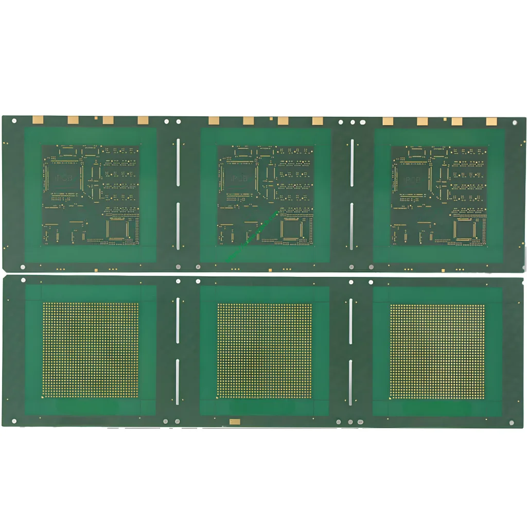
This board, built with SI10U material in a 6-ชั้น (2+2+2) construction and a slim profile of 0.6มม, exemplifies state-of-the-art HDI เทคโนโลยี. ด้วยก 35x35mm unit size, it features a 0.1mm minimum laser via diameter, 30μm minimum trace width / 70μm minimum spacing, และ เกี่ยวกับ enepic (อิเล็กโทรไลต์นิกเกิลอิเล็กโทรไลเซิลแพลเลเดียม) พื้นผิวเสร็จสิ้น, making it an ideal solution for packaging high-speed, ความถี่สูง, and highly integrated chips.
In-Depth Analysis: ออกแบบ, การทำงาน, and Applications
Core Definition & หลักการทำงาน
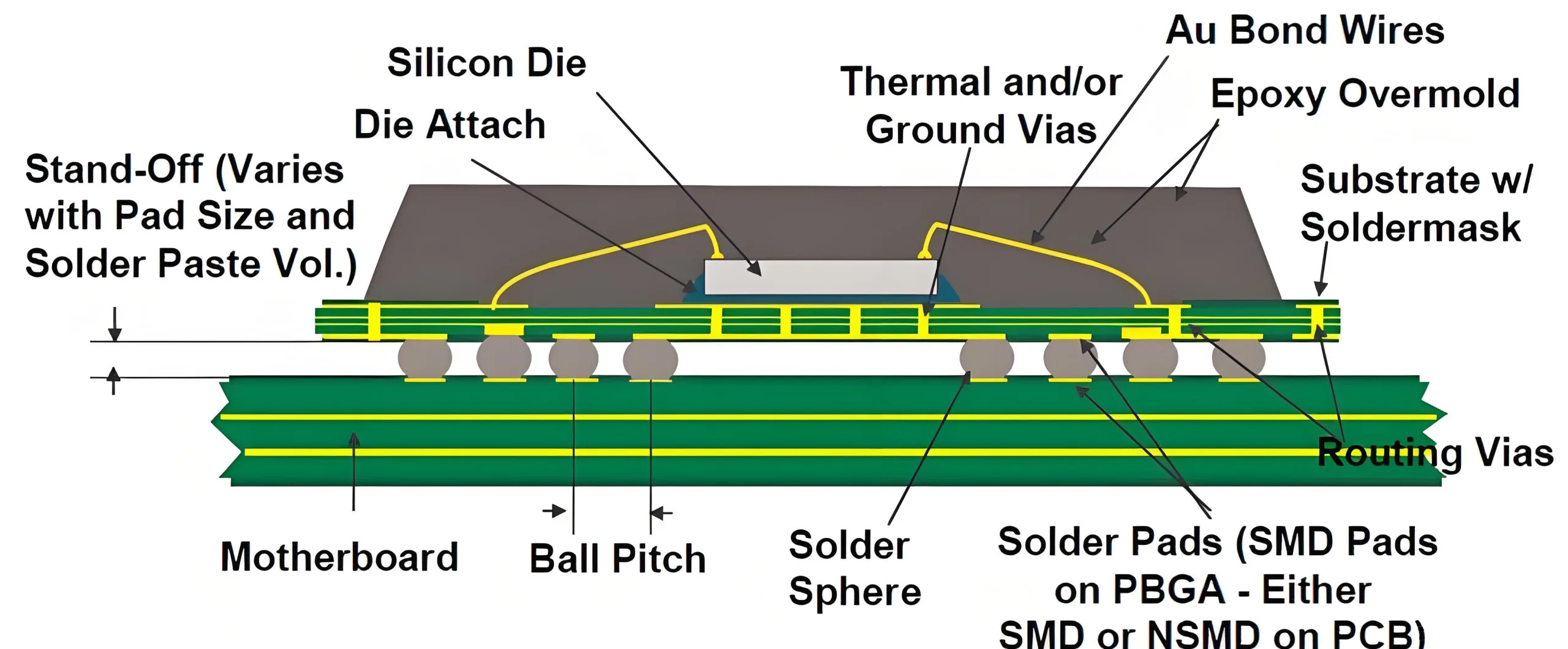
The HDI IC Substrate is designed to “fan-out” the dense array of micro-bumps from a semiconductor die, redistributing the connections to a larger pitch compatible with standard การประกอบ PCB processes like BGA (อาร์เรย์กริดบอล) การติดตั้ง.
The working principle follows this chain: Die → Microbumps → HDI IC Substrate (for signal redistribution & การเชื่อมต่อโครงข่าย) → Solder Balls (บีจีเอ/ซีเอสพี) → Mainboard PCB. It is pivotal for signal integrity, power delivery, และการจัดการความร้อน.
ข้อควรพิจารณาในการออกแบบที่สำคัญ
-
Stack-up & การควบคุมความต้านทาน: The 6-layer (2+2+2) build-up is a classic design for high routing density. Precise impedance calculation (typically 50Ω single-ended or 100Ω differential) is crucial for signal integrity.
-
Micro-via Reliability: 0.1มม (100μm) laser-drilled micro-vias are key for interconnect density. Via shape, copper plating, and fill process must be optimized for thermal cycle reliability.
-
Fine-Line Fabrication: 30μm trace width and 70μm spacing are core metrics of process capability, directly impacting I/O density and electrical performance.
-
Thermal & Mechanical Management: The selection of SI10U material considers its Coefficient of Thermal Expansion (ซีทีอี) matching with silicon to minimize thermal stress and enhance product longevity.
Primary Materials & ลักษณะประสิทธิภาพ
-
Core Material: SI10U. A high-performance laminate offering low dielectric constant (ดีเค), low dissipation factor (ฟ), high glass transition temperature (ทีจี), และความเสถียรของมิติที่ดีเยี่ยม, ideal for high-speed, high-frequency applications.
-
หน้ากากบัดกรี: PSR-4000 AUS308. A high-resolution, high-reliability Liquid Photoimageable Solder Mask (LPSM) that provides precise coverage, excellent insulation, และทนต่อสารเคมี.
-
พื้นผิวเสร็จสิ้น: เกี่ยวกับ enepic. This finish deposits sequential layers of Nickel, Palladium, and Gold. Nickel acts as a diffusion barrier, Palladium prevents nickel corrosion, and the thin gold layer offers superior solderability and wire-bonding capability, perfect for fine-pitch pads.
-
Performance Summary: ความหนาแน่นสูง, ความเร็วสูง, ความน่าเชื่อถือสูง, การจัดการความร้อนที่ยอดเยี่ยม, and superior signal integrity.
การจำแนกประเภท & สถานการณ์การใช้งาน
HDI IC Substrates are categorized by technology and application:
-
โดยเทคโนโลยี: With core (เช่น, this 6L build-up) or coreless types.
-
โดยการสมัคร:
-
Advanced Processors: CPU, GPU, AI accelerator chips requiring maximum routing density and signal speed.
-
Mobile & RF: Smartphone Application Processors (AP) and RF modules, where miniaturization and thin profiles (0.6มม) are critical.
-
หน่วยความจำ: Interface substrates for High Bandwidth Memory (HBM).
-
Networking & เกี่ยวกับยานยนต์: High-speed switch chips and ADAS domain controllers.
-
UGPCB’s Manufacturing Process & การประกันคุณภาพ
UGPCB’s production integrates leading-edge processes compliant with IPC standards:
-
การขุดเจาะเลเซอร์: UV laser systems create precise 0.1mm micro-vias.
-
การชุบ & Via Fill: Advanced pulse plating ensures complete via filling for reliable interconnects.
-
Advanced Imaging: High-end exposure systems and high-resolution dry film achieve 30/70μm line definition.
-
การเคลือบ: Precise alignment and pressing of multiple core layers and prepreg (PP).
-
การตกแต่งพื้นผิว: Application of the เกี่ยวกับ enepic coating for optimal solderability.
-
Comprehensive Testing: Utilizes AOI (การตรวจสอบด้วยแสงอัตโนมัติ), flying probe testing, and impedance testing to guarantee compliance.
ของเรา one-stop พีซีบี service capability extends from สารตั้งต้น IC การผลิต to subsequent แอสเซมบลี SMT และ การทดสอบ, offering a complete packaging solution.
Why Choose UGPCB for Your HDI IC Substrate?
-
Advanced Process Capability: Proven expertise in 30/70μm trace/space และ 0.1mm micro-via เทคโนโลยี.
-
Materials Expertise: In-depth knowledge of advanced materials like SI10U to recommend optimal solutions.
-
Uncompromising Quality: Stringent, automotive-grade quality control throughout the entire process.
-
One-Stop Solution: We are more than a PCB fabricator; we are your PCBA partner, offering design support, การผลิต, และการชุมนุม.
-
Expert Support: Dedicated engineering team provides DFM (ออกแบบเพื่อการผลิต) analysis and technical consultation.
รับโซลูชันที่กำหนดเองของคุณตอนนี้
Whether you are developing the next HPC platform, 5โครงสร้างพื้นฐานจี, หรือ ADAS system, UGPCB’s professional HDI IC Substrate manufacturing และ บริการประกอบ PCBA are your foundation for success.
Contact us today for a free technical consultation and quote! Let our experts help you enhance product performance through optimized IC substrate design and reliable การผลิต PCB กระบวนการ.


