
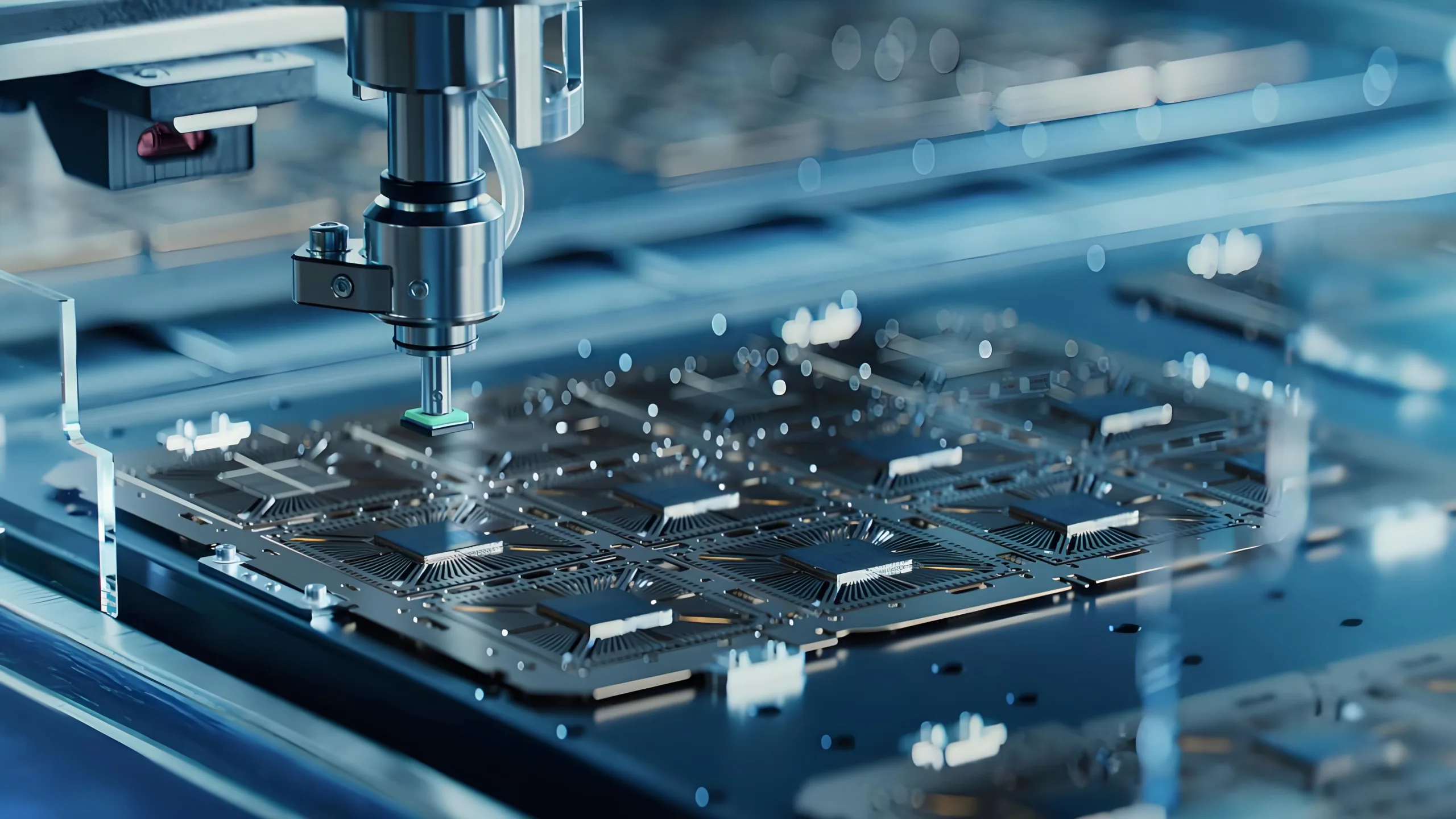
Halbleiterchips dienen als die als die “Gehirn” der digitalen Ära, während die Chipverpackung als ihre Schutzschützerin fungiert “Rüstung” Und “Neurales Netzwerk.” Jenseits der Abschirmung zerbrechlicher Silizium stirbt, Es ermöglicht ein kritisches thermisches Management, elektrische Konnektivität, und Signalübertragung. Von sperrigen Durchläufpaketen bis hin zu Lösungen auf ultradünne Waferebene, Die Verpackungsentwicklung hat die Elektronik -Miniaturisierung und Leistungsverbesserung angetrieben - eine monumentale technologische Saga.
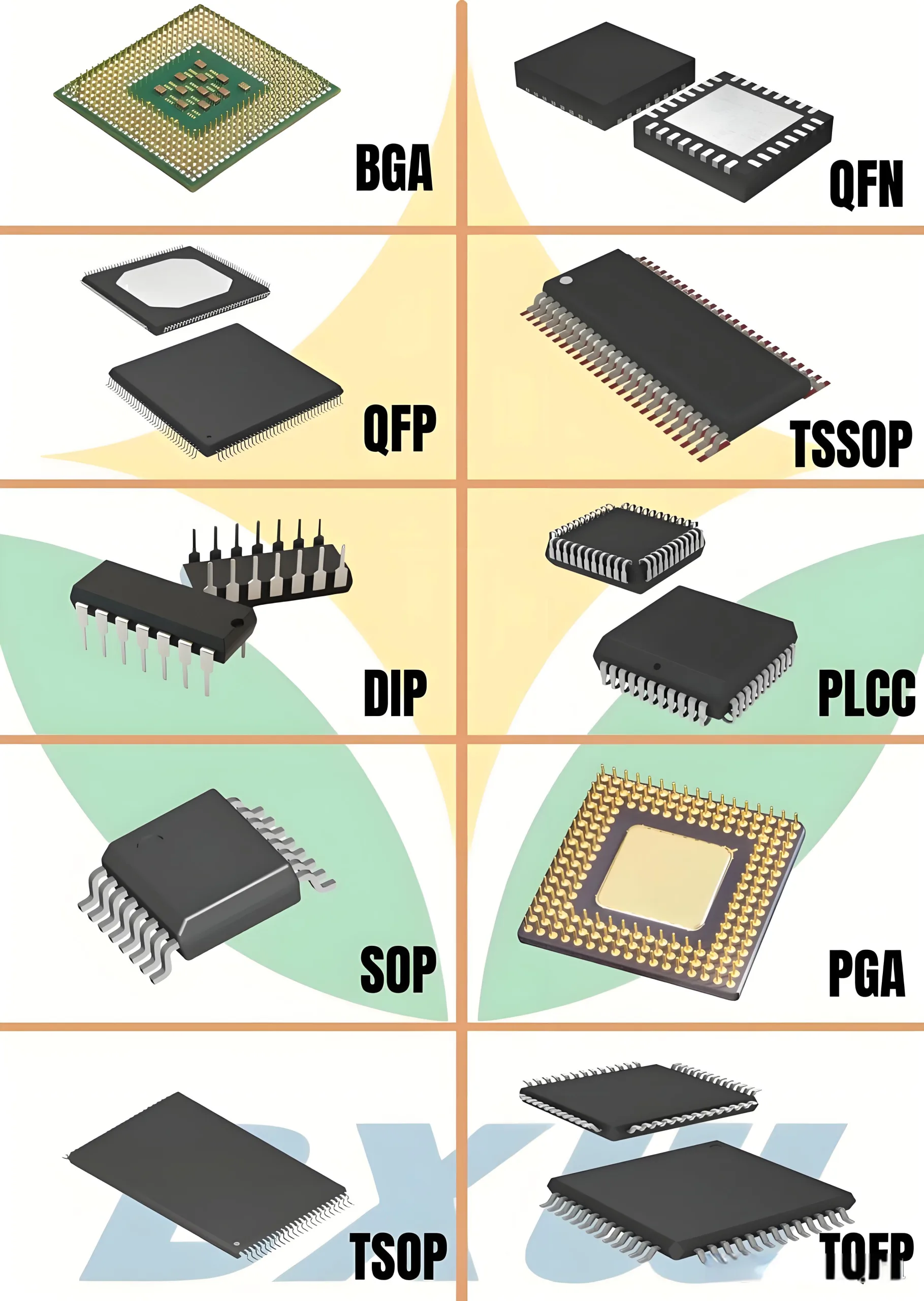
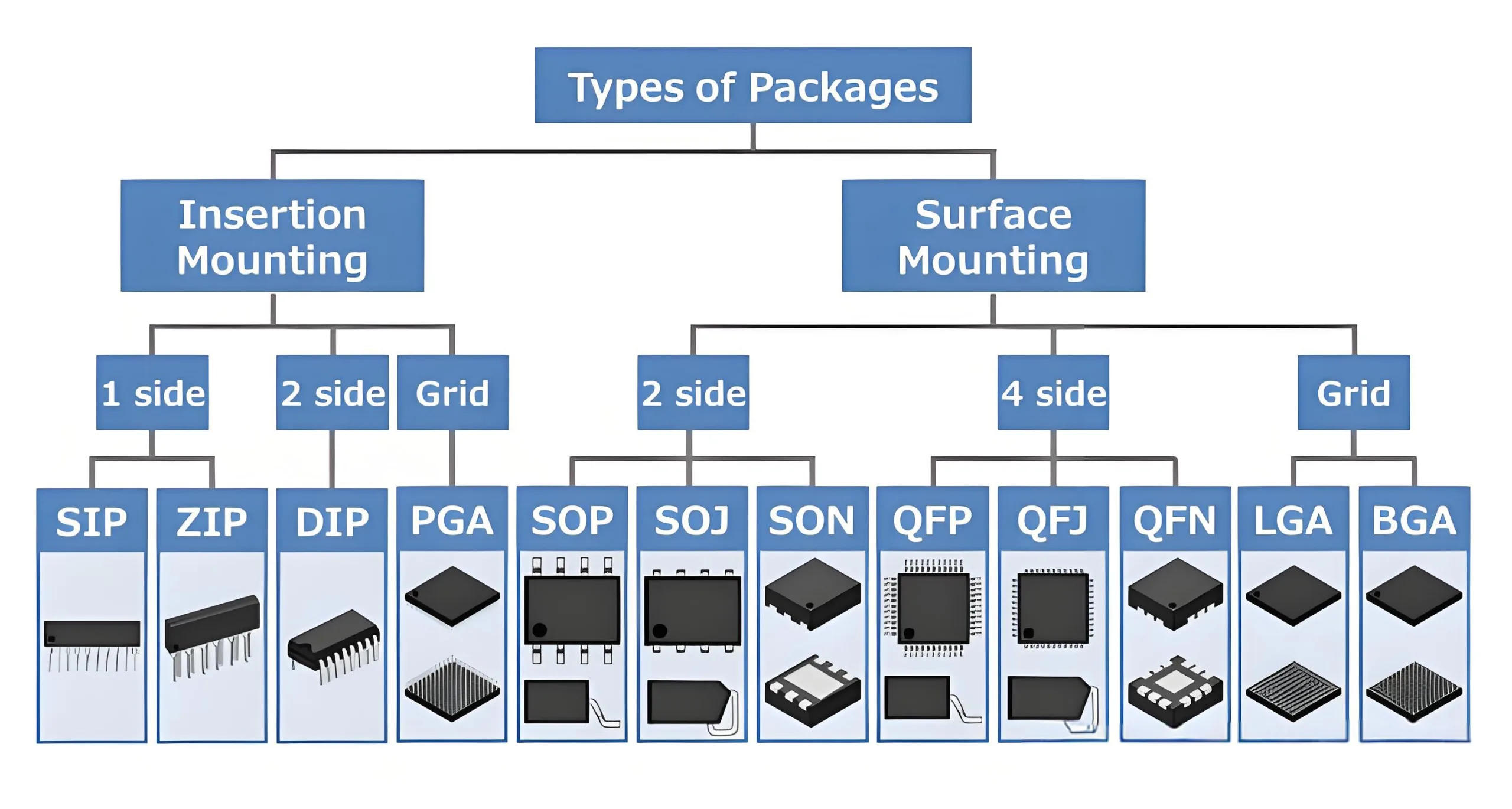
Verpackungstechnologien klassifizieren
Durch Montagemethode
-
Durchleitungsverpackung (Tht):
Stifte eingefügt in Leiterplatte Durchlöten durchlötet. Repräsentiert Technologie der frühen Generation. -
Oberflächenmontechnologie (SMT):
Komponenten, die direkt auf PCB -Pads gelötet wurden. Ermöglicht eine höhere Dichte und automatisierte Baugruppe.
Nach Pinkonfiguration (Dichteentwicklung)
Einzelreihe → Dual-Reis
Die Durchschnitts-Ära
Tun/zu: Grundlagen diskreter Komponenten
-
Do-41 Diode: Ø2,7 mm × 5,2 mm
-
To-220-Transistor: Griffe ≤ 50 W Leistungsdissipation
-
Thermischer Widerstand: R<Sub>Und</Sub> = (T<Sub>J</Sub> – T<Sub>A</Sub>)/P
Wo R<Sub>Und</Sub> = Wärmewiderstand von Junction-to-ambient
SIP/ZIP: Single-in-Line-Innovationen
-
SCHLUCK: 3-16 Stifte, kostengünstig für Widerstände/Dioden mit geringer Leistung
-
REISSVERSCHLUSS: 40% höhere Stiftdichte als SIP über Zick -Zack -Stiftanordnung
-
Anwendungen: Frühe Speichermodule, Spannungsaufsichtsbehörden
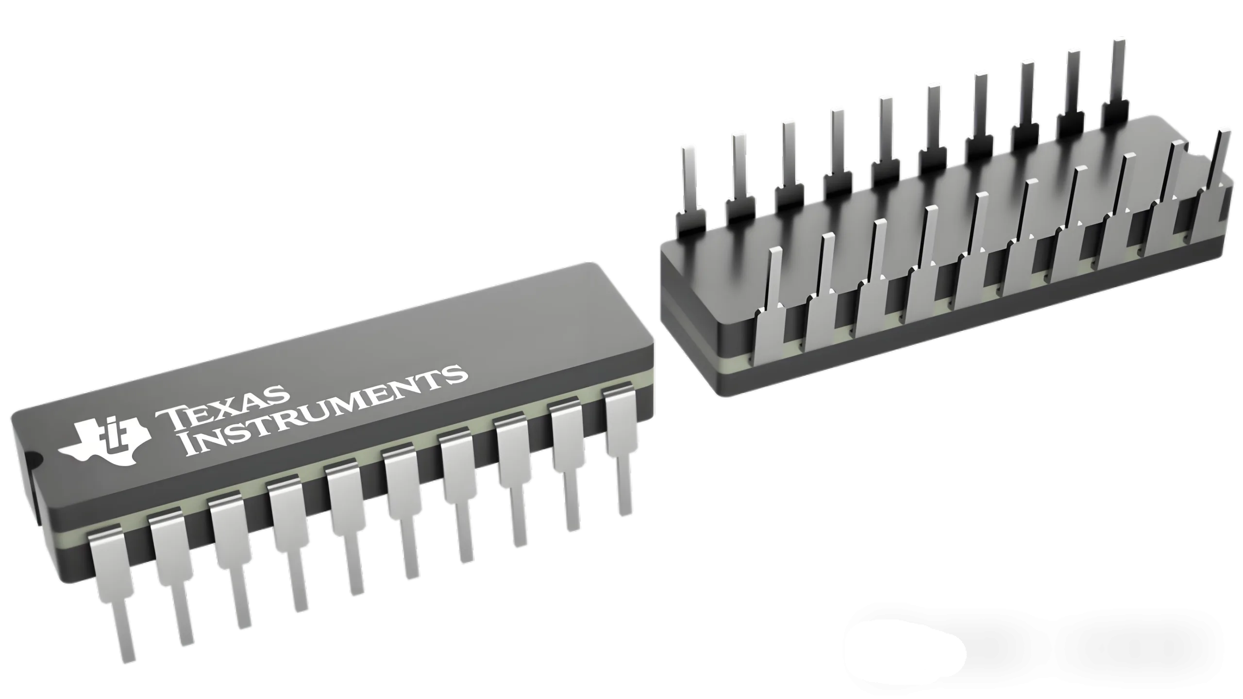
TAUCHEN: Die IC -Revolution
-
Pin -Tonhöhe: 2.54mm (0.1″) Standard
-
1980S Marktanteil: >70% von IC -Verpackung
-
Wärmeleistung:
Keramikdip: 20-30 W/M · k -Leitfähigkeit
Plastikdip: 0.2-0.3 W/m · k
PGA: Hochleistungs-Computing Pioneer
-
Pindichte: 3× höher als Dip
-
Anwendungen: Intel 80386/80486 CPUs
-
Einfügungskraft: 30-100 Newtons
Die SMT -Revolution
SOD/SOT: Diskrete Komponentenminiaturisierung
-
SOD-323: 1.7mm × 1,25 mm
-
SOT-23 Wärmewiderstand: ~ 250 ° C/W.
-
Reflow -Profil: Peak Temp 235-245 ° C.
Möwenflügel führt: SOP -Familie
-
Pin -Tonhöhe Evolution:
1.27mm (SOP) → 0,8 mm (SSOP) → 0,65 mm (TSSOP) -
Ableitungspakete:
SOP → SSOP → TSOP → TSSOP → VSSSOP -
Wärmeverstärkung: HSSOP reduziert den thermischen Widerstand durch 40%
J-Lead-Konfiguration: Beobachtung
-
Mechanische Stärke: 30% höherer Stresswiderstand
-
Elektrische Einschränkung: 0.8-1.2NH parasitäre Induktivität
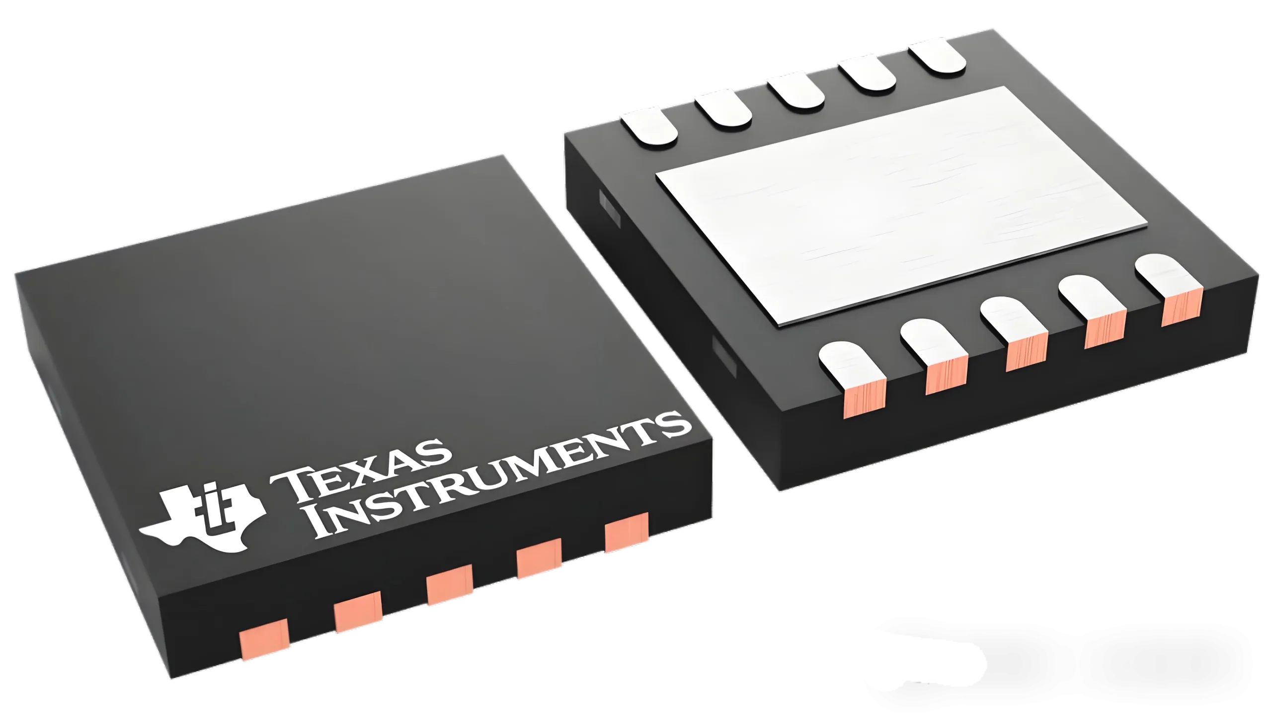
Leadless -Durchbruch: Sohn/DFN
-
Raumeffizienz: >50% Verbesserung gegenüber SOP
-
Wärmeleistung: 15° C/w mit Wärmekissen
-
Miniaturisierungsgrenze:
X2son: 0.6mm × 0,6 mm × 0,32 mm
Physik hinter der Miniaturisierung
Drei Kernherausforderungen regeln das Verpackungsskaling:
-
Thermalmanagement:
Q = haδt
Reduzierte Größe (↓ a) erfordert einen höheren Konvektionskoeffizienten (↑ h) -
Wärmespannungskontrolle:
S = ERTHT
Wo cte (A) Fehlanpassung verursacht Stress -
Signalintegrität:
Bleiinduktivität *l ≈ 2l(ln(2L/d)-1) NH*
Die Miniaturisierung verringert die Induktivität durch 30%
Nächste Grenze: Erweiterte Verpackung
Als X2SON trifft 0,6 mm Skalen, Innovation verlagert sich auf:
-
3D Verpackung: TSV-fähige vertikale Integration
-
Heterogene Integration: Multi-Knoten-Würfelbaugruppe
-
Photonik: Co-Design of Silicon Photonics
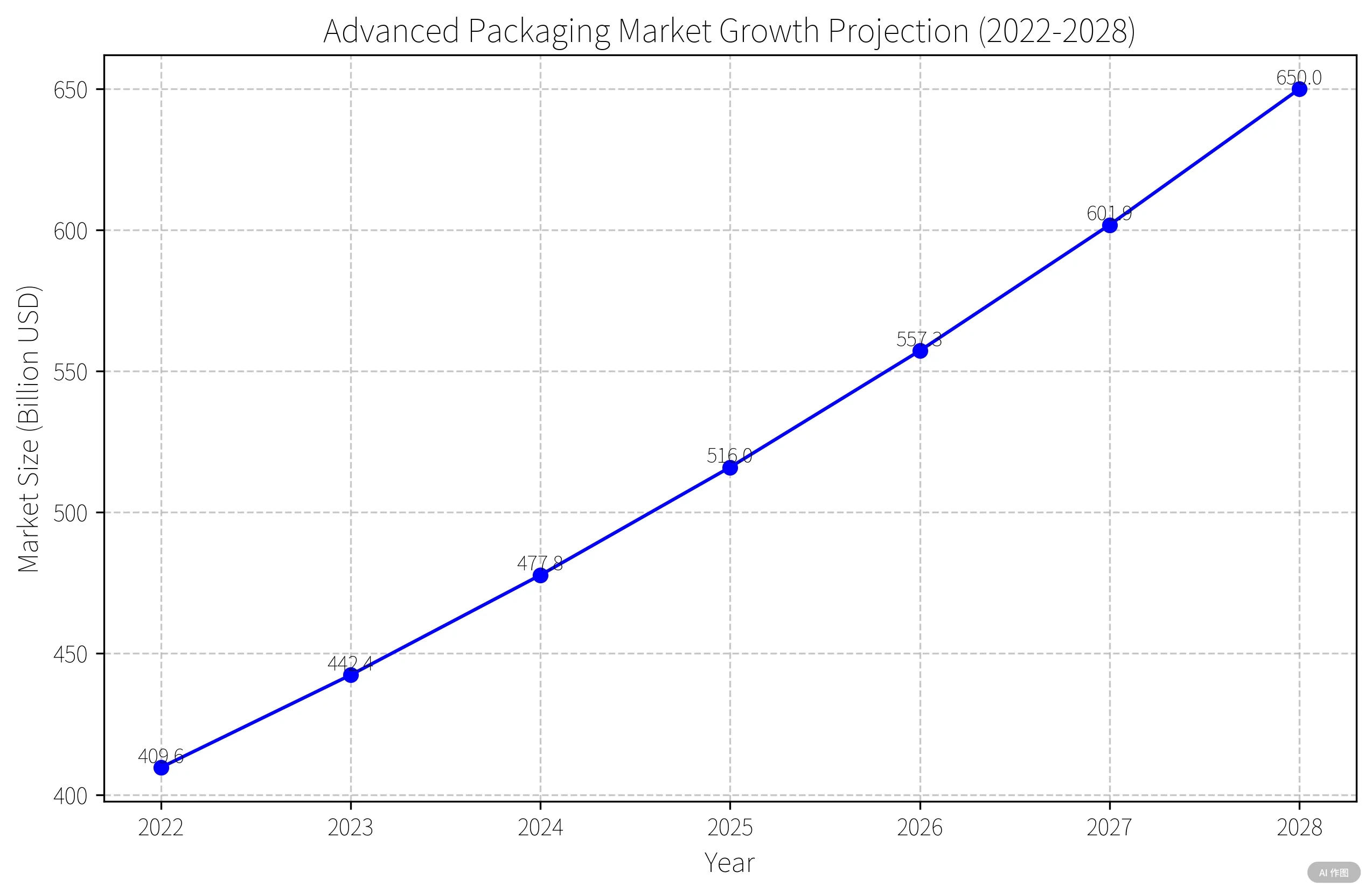
Marktprognose (Yole Dévelcpement):
8% Cagr durch 2028 → 65 -Dollar -Markt
Die Verpackung definiert jetzt die Systemleistung kritisch - weit über den bloßen Schutz hinaus.
Abschluss
Von der 2,54 -mm -Tonhöhe von DIP bis zum 0,6 -mm -Fußabdruck von X2son, Verpackung Fortschritte definieren die Elektronik kontinuierlich neu. Jedes Slim Smartphone und 5G -Gerät stützt sich auf diese unsichtbaren Innovationen. Mit KI und Quantencomputer entstehen, Die Chipverpackung überschreitet weiterhin nanoskalige Grenzen.
*Als nächstes in Serie:
BGA/CSP/WLCSP -Technologien
3D Verpackung & TSV -Verbindungen
Fortgeschrittene Verpackungsmaterialienwissenschaft
Bleiben Sie dran!*
