
Der Kampf um Leben und Tod in der Mikroelektronik: Durch Lötstoppmaskenspalte induzierte Kettenreaktion
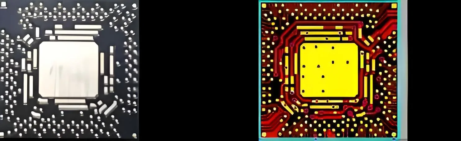
Mit 0201 Komponenten und 0,3-mm-BGAs werden zum Mainstream, Leiterplatte Pad-Lot-Skipping-Raten sind gestiegen 37% (IPC 2023 Daten). Laut einer jahrzehntelangen Studie von UGPCB: 60% der SMT-Defekte sind auf fehlerhafte Pastenübertragung zurückzuführen, Wo Lücken im Mikrotampondruck als der Übersehene agieren “unsichtbarer Mörder”.
Mit Blut geschriebene Lektionen: Mikrograph deckt Schwachstellen der Branche auf
-
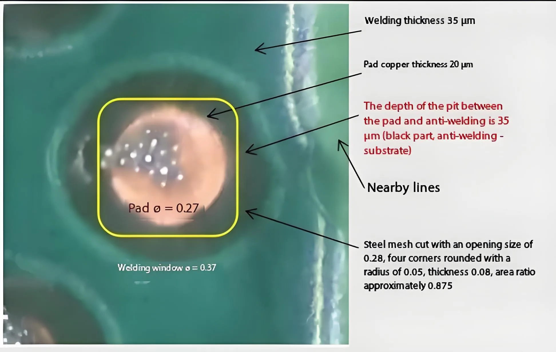
Höhenunterschied zwischen Lötmaske und Kupferpad: 35μm
-
Schablonenöffnung, die den Substratbereich abdeckt: 42%
-
Effektive Lötpasten-Kontaktfläche: <58%
Physik hinter dem Scheitern: Das Mathematische “Todesdreieck” des Pastentransfers
Fatale Formel: Der Zusammenbruch der IPC-7525-Flächenverhältnistheorie
Flächenverhältnis = (L×B) / [2H(L+W)]
Die traditionelle Theorie versagt, wenn der Pad-Durchmesser ≤ 0,3 mm ist! Empirische Daten führender Hersteller verraten es:
| Pad-Durchmesser (mm) | Theoretisches Flächenverhältnis | Tatsächliche Übertragungsrate |
|---|---|---|
| 0.40 | 0.68 | 92% |
| 0.31 | 0.61 | 85% |
| 0.27 | 0.55 | 63% |
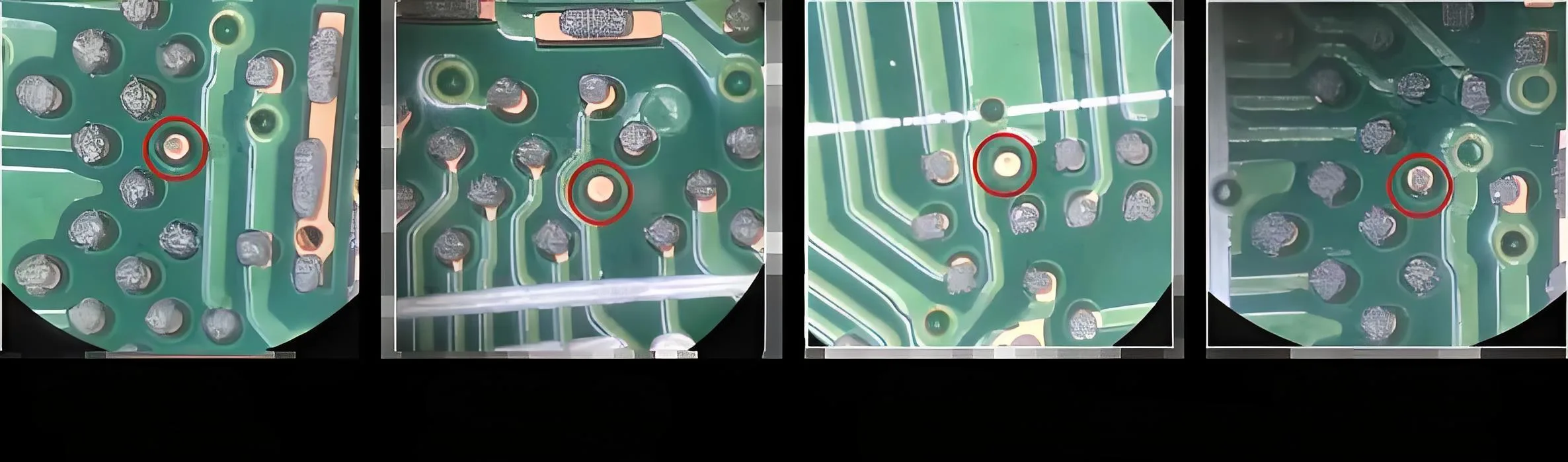
Fluiddynamik offengelegt: Warum Lotpaste “Ausschuss” Polster
Figur 2: Simulation der Flüssigkeitsspannung während der Schablonenfreigabe
Alt: Analyse der Wandspannung von Lotpastenschablonen – Simulation von PCBA-Druckfehlern – SMT-Lösungen
Kritische Erkenntnisse:
-
Lücken in der Lötmaske erzeugen einen Luftpolstereffekt, Reduzierung der Kontaktfläche um 41%
-
Bei der Pastenkohäsion kommt es zu Lötausbrüchen > Pad-Haftung
Lösungen auf Industrieniveau: Drei Säulen zur Vermeidung von Lötausfällen
Pad-Design-Revolution: Prinzip der Kupferexpansion
-
Isolierter Pad-Durchmesser: 0.27mm → 0,31 mm
-
Lückenabdeckung reduziert auf 12%
-
Übertragungsrate erhöht auf 89% (empirische Daten)
Lötmaske “Abnehmen” Initiative: Der 25μm Goldstandard
Figur 3: Druckvergleich mit unterschiedlichen Lötstopplackdicken
Alt: Vergleich der PCB-Lötmaskendicke – Verbesserung der SMT-Ausbeute – Leitfaden für PCBA-Lieferanten
Dickenformel: H = (Rz + D) × K
(δ = Partikelgröße der Paste, Typ 4: 25μm; K = Sicherheitsfaktor 1.2)
Branchenvalidierung: Der Hersteller mobiler Leiterplatten reduzierte die Dicke von 35 μm auf 22 μm → 82% Reduzierung des QFN-Lötsprungs
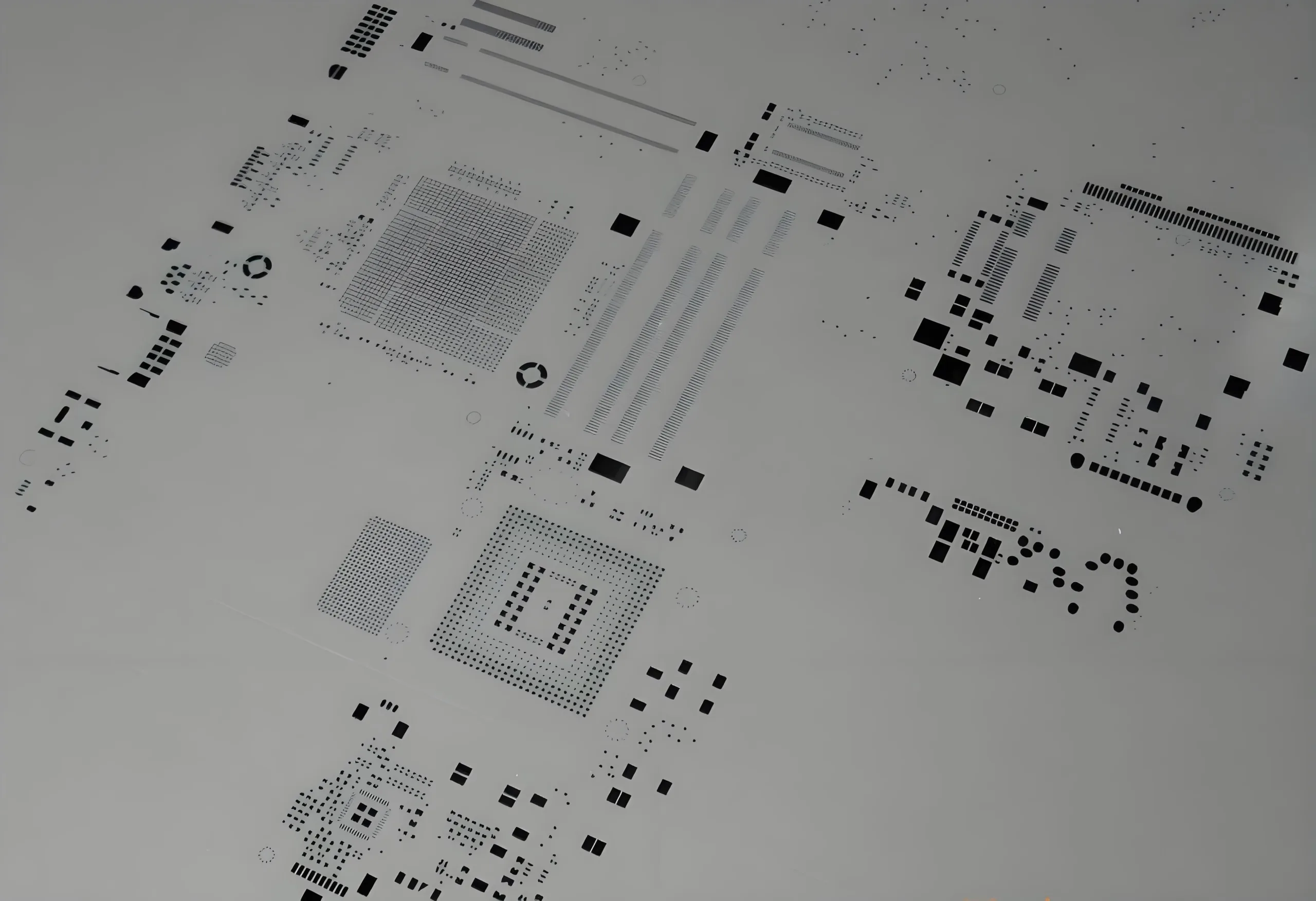
PH-Schablonen: Die ultimative Nano-Konformitätslösung
 Innovationen:
-
Abgestuftes Blendendesign: Wandwinkel von 7° bis 15°
-
Elektrogeformtes Nickel: 3x Härteanstieg
-
Entformungshilfewinkel: 40% reduzierte Wandreibung
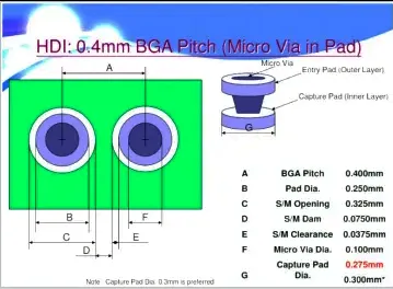
Branchenführer’ Spielbuch: HDI + NSMD-Goldstandard
Die Präzisionsstrategie der Mobilfunkbranche
Fall: 0.4BGA-Prozessplan mit mm-Pitch
1. Legendendruck ersetzen → Design aus blankem Kupfer
2. Implementieren HDI Mikrodurchkontaktierungen
3. Dicke der Lötstoppmaske: 18±3μm (IPC-6012 Klasse 3 konform)
Konvertierungs-Engine: Ihr Aktionsplan für Fabrik-Upgrades
Checkliste für die sofortige Ausführung:
-
Überprüfen Sie alle isolierten Pads: Bei Durchmesser neu konstruieren <0.3mm
-
Fordern Sie Berichte zur Lötstopplackdicke von an PCB -Lieferanten (Schlüsselmetrik: ≤25μm)
-
Besorgen Sie sich dringend PH-Schablonen: 55% Apertureffizienzgewinn in feinen Bereichen
