
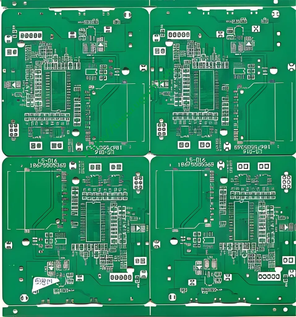
Einführung in die 18Layers Communication Base Station PCB
Die 18Layers Communication Base Station PCB ist hochentwickelt und leistungsstark Leiterplatte speziell für den Einsatz in Kommunikationsbasisstationen entwickelt. Das Leiterplatte bietet außergewöhnliche Haltbarkeit, Zuverlässigkeit, und Effizienz, Dies macht es zur idealen Wahl für kritische Kommunikationsinfrastrukturanwendungen.
Hauptmerkmale und Spezifikationen
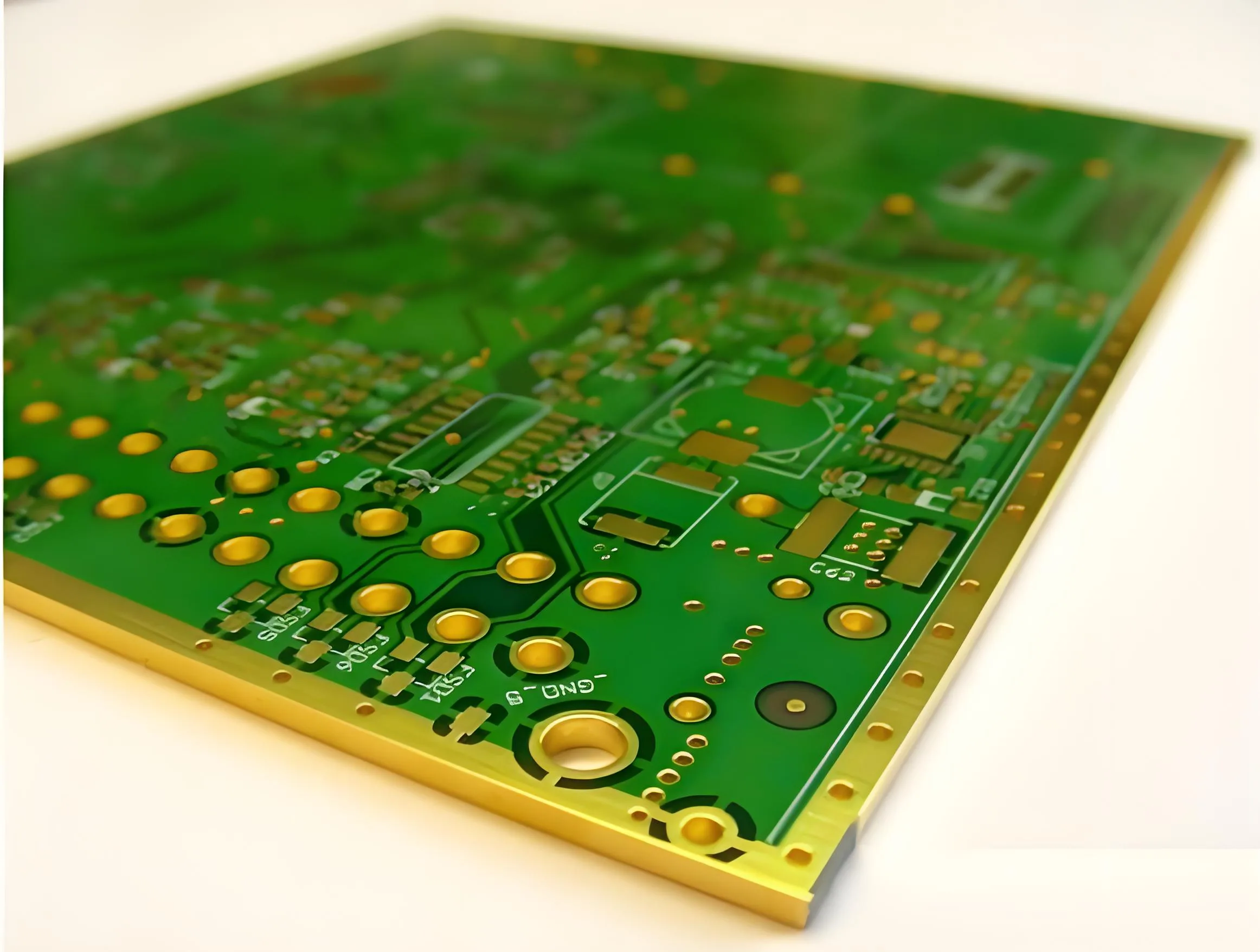
Material
- Material: Die Platine besteht aus Panasonic M6, ein hochwertiges Material, das für seine hervorragenden elektrischen Eigenschaften und thermische Stabilität bekannt ist. Dadurch wird sichergestellt, dass die Leiterplatte rauen Umgebungsbedingungen standhält und eine optimale Leistung beibehält.
Schichten und Kupferdicke
- Schichten: Mit 18 Schichten, Diese Leiterplatte bietet viel Platz für komplexe Schaltungsdesigns, die in fortschrittlichen Kommunikationssystemen erforderlich sind.
- Kupferdicke: Die Kupferdicke reicht von 0.5 Zu 1 oz, Dies ermöglicht eine robuste Signalübertragung und Stromverteilung auf der gesamten Platine.
Abmessungen und Oberflächenbehandlung
- Fertige Dicke: Die Leiterplatte hat eine Enddicke von 2,0 mm, was für strukturelle Integrität und mechanische Festigkeit sorgt.
- Oberflächenbehandlung: Es verfügt über eine Immersionsgold-Oberflächenbehandlung. Dies steigert nicht nur die Ästhetik, sondern verbessert auch die Lötbarkeit, Korrosionsbeständigkeit, und Kontaktsicherheit.
Präzises Design
- Spur/Raum: Mit präzisen Spur-/Raummessungen von 4mil/4mil (0.1Mm/0,1 mm), Diese Leiterplatte gewährleistet eine hochdichte Interkonnektivität mit minimalem Übersprechen und Signalverlust.
- Min -Loch: Die minimale Lochgröße beträgt 0,2 mm (8Mil), Dies ermöglicht Fine-Pitch-Komponenten und Layouts mit hoher Dichte.
Besondere Prozesse
- Spezialprozess: Die Leiterplatte verfügt über einen Metallkantenprozess, was den Kanten zusätzliche Festigkeit und Schutz verleiht, Verbesserung der allgemeinen Haltbarkeit und Lebensdauer des Boards.
Anwendungen
Die 18Layers-Kommunikationsbasisstationsplatine wird hauptsächlich in Kommunikationsbasisstationsanwendungen verwendet, bei denen hohe Zuverlässigkeit und Leistung von entscheidender Bedeutung sind. Dazu gehören:

- Basisstationen für Mobilfunknetze
- Radiofrequenz (Rf) Transceiver
- Mikrowellenkommunikationssysteme
- Netzwerkgeräte für Rechenzentren
Produktionsprozess
Der Herstellungsprozess der 18Layers Communication Base Station PCB umfasst mehrere sorgfältige Schritte, um höchste Qualitätsstandards zu gewährleisten:
- Materialauswahl: Hochwertige Panasonic M6 Material wird aufgrund seiner hervorragenden elektrischen Eigenschaften und Haltbarkeit ausgewählt.
- Schichtstapel: Der 18 Die Schichten werden sorgfältig gestapelt und mithilfe fortschrittlicher Laminiertechniken miteinander verbunden.
- Ätzen und Bohren: Präzise Ätz- und Bohrprozesse erzeugen die komplizierten Schaltkreismuster und Löcher, die für die Komponentenplatzierung erforderlich sind.
- Beschichtungs- und Lötmaskenanwendung: Die abschließende Oberflächenbehandlung erfolgt durch Tauchvergoldung und Auftragen einer Lötstoppmaske, Gewährleistung einer hervorragenden Leitfähigkeit und Schutz vor Umwelteinflüssen.
- Qualitätskontrolle: Jede Leiterplatte wird strengen Tests und Inspektionen unterzogen, um strenge Qualitätskriterien zu erfüllen, bevor sie für den Versand verpackt wird.

Abschluss
Die 18Layers Communication Base Station PCB ist ein hochspezialisiertes Produkt, das den anspruchsvollen Anforderungen moderner Kommunikationsinfrastruktur gerecht wird. Seine fortschrittlichen Materialien, Präzisionsdesign, und strenge Herstellungsprozesse machen es zu einer zuverlässigen Wahl für jedes leistungsstarke Kommunikationssystem. Ganz gleich, ob Sie Mobilfunkbasisstationen oder Rechenzentrumsausrüstung bauen, Diese Leiterplatte bietet unübertroffene Zuverlässigkeit und Leistung.


