UGPCB 26-lagige Hochleistungs-Serverplatine: Die zentrale Grundlage für die Rechenleistung von Rechenzentren
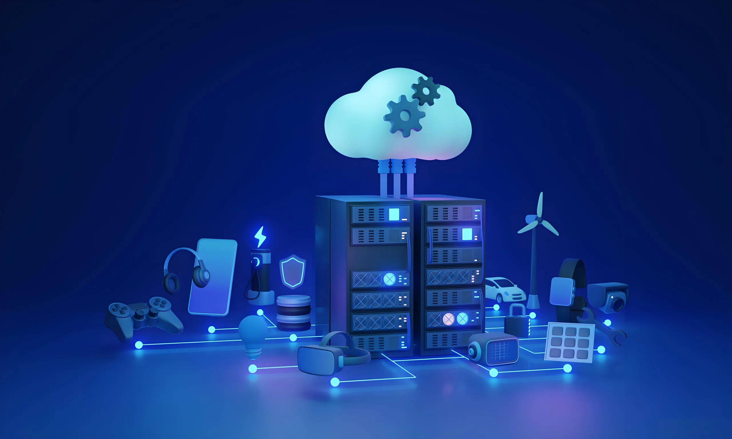
Im digitalen Zeitalter, Server sind die “Supergehirne” Verarbeitung riesiger Datenmengen, und die Server Leiterplatte (Leiterplatte) ist das Kritische “Neurales Netzwerk” dieses Gehirns. Ein gut gestaltetes, Präzise gefertigtes High-End Server-Motherboard-PCB bestimmt direkt die Verarbeitungsgeschwindigkeit eines Rechenzentrums, Energieeffizienz, und langfristige Betriebsstabilität. Nutzung umfassender Fachkenntnisse in hohe Geschwindigkeit, High-Layer-Count Leiterplattenherstellung, UGPCB hat dieses Flaggschiff entwickelt 26-Layer-Server-PCB für Hochleistungsrechnen der nächsten Generation (HPC), AI -Server, und Cloud-Rechenzentren. Es wurde entwickelt, um eine außergewöhnliche elektrische Leistung und eine zuverlässige physikalische Struktur zu liefern, um extreme Rechenlasten zu unterstützen.
Produktdefinition & Überblick: Was ist eine High-End-Serverplatine??
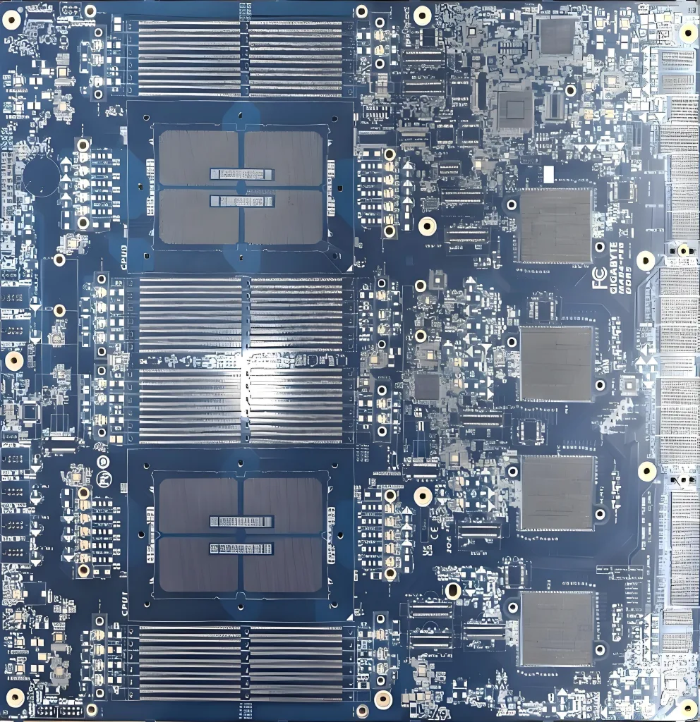
Eine High-End-Serverplatine ist komplex, Mehrschichtige Leiterplatte zur Aufnahme von Kernkomponenten wie CPUs, Erinnerung, Hochgeschwindigkeitsschnittstellen (z.B., PCIE, CXL), und Power-Management-Einheiten, und Ultrahochgeschwindigkeit zu etablieren, äußerst zuverlässige elektrische Verbindungen zwischen ihnen. Es handelt sich nicht nur um ein mechanisches Substrat, sondern um eine entscheidende Plattform zur Gewährleistung der Signalintegrität und Leistungsintegrität bei GHz-Frequenzen. Das UGPCB Produkt verfügt über eine anspruchsvolle 26-Layer-PCB-Aufbau, Verwendung fortschrittlicher Materialien und Prozesse, die speziell für anspruchsvolle Anwendungen wie Big-Data-Verarbeitung und KI-Training entwickelt wurden.
Kernpunkte des Designs & Arbeitsprinzip
Die Hauptfunktion einer Server-Leiterplatte besteht darin, eine verlustarme Schaltung bereitzustellen, störungsarmer Übertragungsweg für Hochgeschwindigkeits-Digitalsignale und Hochstrom-Stromversorgung. Sein Design basiert auf mehreren Grundprinzipien:
-
Signalintegrität (UND): Die Verwendung von Hochgeschwindigkeitsmaterialien (Tg 170) und präzise Kontrolle über Spurbreite/Abstand von 0,08 mm/0,09 mm minimiert Signaldämpfung und Verzerrung, Gewährleistung einer fehlerfreien Datenübertragung mit Raten von mehreren zehn Gbit/s.
-
Kraftintegrität (PI): Die Eingliederung von 2Unze schweres Kupfer (2/2 oz) für Strom und interne Ebenen reduziert den Gleichstromwiderstand und den Temperaturanstieg, Bereitstellung ausreichender und sauberer Energie für leistungsstarke Chips wie CPUs/GPUs.
-
Impedanzkontrolle & Kulisse: Auf Hochgeschwindigkeitskanäle wird eine strenge Impedanzkontrolle angewendet. Eine Schlüsselinnovation ist der Einsatz von Hinterbohrtechnik um den unbenutzten leitfähigen Stutzen zu entfernen (Fass) von plattierten Durchgangslöchern, Eliminieren von Signalreflexionspunkten – ein zentraler Prozess zur Verbesserung Signalqualität in Hochgeschwindigkeits-PCBs.
-
Thermalmanagement & Zuverlässigkeit: A fertige Plattenstärke von 2,97 mm ±10 % Und hohe Tg 170 Material bieten hervorragende mechanische Festigkeit und Hitzebeständigkeit, Sicherstellen, dass die Leiterplatte auch unter längeren Bedingungen stabil und zuverlässig bleibt, hohe Temperatur, Volllastbetrieb von Servern.
Technische Spezifikationen & Materialien
-
Schichtzahl & Dicke: 26 Schichten, Dicke der fertigen Platte 2.97mm ±10 %.
-
Stapelung von Kupfergewichten: Komplexe Konfiguration: 1/1/H/1/H/1/H/1/H/1/H/2//2/2/H/1/H/1/H/1/H/1/H/1/1 oz. Verwendung kritischer Leistungsschichten 2Unze schweres Kupfer um Signal- und Leistungsbedarf auszugleichen.
-
Kernmaterial: Taiyao TU883 hohe Geschwindigkeit, verlustarmes Laminat mit a Glasübergangstemperatur (Tg) von 170°C. Es bietet eine sehr niedrige Dielektrizitätskonstante (Dk) und Verlustfaktor (Df), Dies macht es zu einer erstklassigen Wahl für Hochgeschwindigkeits-PCB-Materialien.
-
Linienpräzision: Mindestspurbreite/-abstand von 0.08mm / 0.09mm, Ermöglicht Routing mit hoher Dichte.
-
Micro-Via-Technologie: Unterstützt a minimaler mechanischer Bohrerdurchmesser von 0,20 mm, Treffen mit hoher Verbindungsdichte (HDI) Anforderungen.
-
Oberflächenbeschaffung: Bio -Lötlichkeitsschutz (OSP) bietet eine Wohnung, Hochlötbare Oberfläche für Hochleistungs-BGA und Chip Komponenten, bietet eine hervorragende Wirtschaftlichkeit.
Produktklassifizierung, Struktur & Merkmale
-
Wissenschaftliche Klassifikation: Dieses Produkt gehört zur Kategorie von “High-End-Mehrschicht-Hochgeschwindigkeits-Server-Motherboard-Leiterplatten”, speziell “Hoher Tg, Hohe Schichtanzahl, Hinterbohrt, Power-Delivery-Leiterplatten aus schwerem Kupfer”.
-
Kernstrukturmerkmale:
-
Mehrschichtige Laminierung: Präzise Signalanordnung, Boden, und Leistungsebenen sorgen für eine wirksame elektromagnetische Abschirmung und Rückwege mit niedriger Impedanz.
-
Backdrill-Struktur: Durchgangslöcher für kritische Hochgeschwindigkeitsverbindungen (z.B., PCIe-Lanes, Speichersteckplatzanschlüsse) sind hinterbohrt, um die Hochfrequenzleistung deutlich zu verbessern.
-
RTF-Kupferfolienanwendung: Die Verwendung von umgekehrt behandelter Folie sorgt für eine glattere Kupferoberfläche, Dadurch wird der Signalverlust während der Übertragung entlang des Leiters weiter reduziert.
-
Strenger Produktionsprozess
Der Herstellungsprozess von UGPCB folgt strikt der IPC-A-600G/6012-Klasse 2/3 Standards, mit erweiterten Steuerungen für Server-PCBs:
Materialschneiden → Bildgebung der inneren Schicht & AOI-Inspektion → Laminierung & Bohren → Stromlos & Elektrolytische Kupferabscheidung → Backdrilling-Prozess → Bildgebung der Außenschicht → Sekundäres AOI & Impedanzprüfung → Lötmaske & OSP-Anwendung → Elektrischer Test (Fliegende Sonde/Testvorrichtung) → Abschließende Sichtprüfung & Verpackung.
Unter diesen, Hinterbohren Und Impedanztest sind kritische Kontrollpunkte, die die Qualität sicherstellen Hochleistungs-Serverplatine.
Zielanwendungen
Dieses Produkt wurde speziell für die folgenden High-End-Anwendungen entwickelt und hergestellt:
-
Künstliche Intelligenz & Server für maschinelles Lernen: Hosten von Trainings- und Inferenz-GPU/ASIC-Clustern.
-
Cloud Computing & Rechenzentrumsserver: Für Hochleistungsrechnen (HPC) Cluster und Virtualisierungshosts.
-
Enterprise-Speicherserver: Speichergeräte, die eine hohe Zuverlässigkeit und zahlreiche Hochgeschwindigkeits-Datenschnittstellen erfordern.
-
5G-Core-Netzwerkausrüstung: Netzwerkinfrastruktur für Hochgeschwindigkeits-Datenvermittlung.