

Kundenspezifische 2-lagige starre FR-4-Leiterplatte: ZUSTIMMEN + Hartgold-Finish für hohe Zuverlässigkeit & Kosteneffizienz
Entdecken Sie die Branche “Goldstandard” für ausgewogene Leistung und Erschwinglichkeit. UGPCBs 2-lagiges starres FR-4 Leiterplatte, mit TG150-Hochtemperaturmaterial und einer doppelten ENIG + Oberfläche aus Hartgold, bietet überragende Zuverlässigkeit für anspruchsvolle Anwendungen.
ICH. Warum sollten Sie sich für eine 2-lagige starre FR-4-Leiterplatte entscheiden??
Im Zeitalter der elektronischen Miniaturisierung, die Nachfrage nach hohe Zuverlässigkeit, niedrige Kosten, Und kompaktes Design hat die 2-lagige starre Leiterplatte hergestellt “goldene Wahl” für Ingenieure und Einkaufsmanager. Im Gegensatz zu einseitigen Platinen mit eingeschränktem Routing-Platz oder teuren Mehrschichtplatinen, Das 2-Lagen-Design bietet die perfekte Balance zwischen Leistung und Preis.
UGPCB verbessert diese Basis durch die Nutzung FR-4 TG150 hitzebeständiges Material und ein spezialisierter Elektrololes Nickel -Eintauchgold (ZUSTIMMEN) + Hartes Gold Oberflächenbehandlung. Diese Kombination verbessert die Haltbarkeit und Lötbarkeit erheblich, Dadurch eignet es sich für ein breiteres Spektrum rauer Umgebungen.
II. Produktkernspezifikationen (IPC-A-600-konform)
Die folgenden Parameter gewährleisten volle Kompatibilität mit Industriestandards und optimale Herstellbarkeit (DFM).
| Parameter | Spezifikationsdetails |
|---|---|
| Schichtzahl | 2 Schichten (Doppelseitig: Spitze & Bodenführung, FR-4-Kernsubstrat) |
| Brettdicke | 1.60mm (Standardstärke in der Industrie, Ausgleich der mechanischen Festigkeit & Raum) |
| Grundmaterial | FR-4 TG150 (Glasgewebe aus Epoxidharz; Glasübergangstemp: 150°C; Hervorragende Hitzebeständigkeit) |
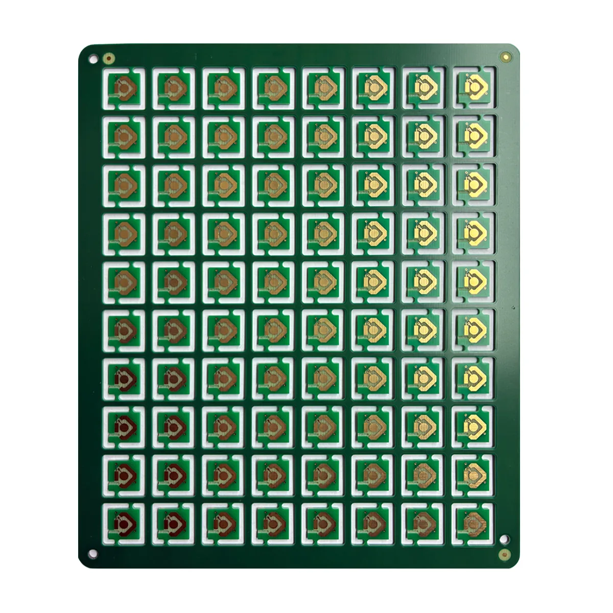
| Oberflächenbeschaffung | JEDE 2h” + Hartgold 30u” (Doppelter Schutz: Chemisches Immersionsgold + Galvanisiertes Gold für Verschleißfestigkeit) |
| Kupfergewicht | 1oz (35μm) (Standarddicke, ausreichend für die meisten aktuellen Trageanforderungen) |
| Lötmaske | Grün (Standard; Schwarz, Blau, Rot, Weiß auf Anfrage erhältlich) |
| Siebdruck | Weiße Epoxidtinte (Komponentenbezeichner, Logo) |
| Min. Loch bohren | 0.3mm (12Mil) |
| Min. Linienbreite/Abstand | 3Mil / 3Mil |
III. Produktdefinition: Was ist eine 2-lagige starre Leiterplatte??
1. Definition
A Starre PCB ist eine nicht flexible Leiterplatte, die aus einem Substrat besteht, Kupferfolienspuren, Lötmaske, und Siebdruck. Durch Bohr- und Ätzprozesse werden feste elektrische Verbindungen hergestellt.
A 2-Schichtstarre Leiterplatte (Doppelseitiges Brett) ist der grundlegende Typ der starren Leiterplatte, mit Kupferspuren sowohl auf der Ober- als auch auf der Unterseite des Substrats. Elektrische Verbindungen zwischen den Schichten werden über erreicht Durchkontaktierte Löcher (Vias).
2. Klassifizierung nach Layeranzahl
- 1-Schicht (Einseitig): Schaltungen nur auf einer Seite. Niedrigste Kosten, aber erhebliche Routing-Einschränkungen.
- 2-Schichten (Doppelseitig): Schaltungen auf beiden Seiten. Höhere Routing-Flexibilität als einseitig; moderate Kosten. (Die Spezialität von UGPCB)
- Mehrschichtig (4+ Schichten): Drei oder mehr Kupferschichten. Geeignet für komplexe Schaltungen, aber deutlich höhere Kosten.
Das 2-Layer-Angebot von UGPCB repräsentiert das höchstes Preis-Leistungs-Verhältnis in der Kategorie starre Leiterplatten.
IV. Designrichtlinien für hohe Zuverlässigkeit
Mit begrenztem Routing-Platz auf 2-Lagen-Platinen, Halten Sie sich an IPC-2221 Designstandards sind für die Signalintegrität und das Wärmemanagement von entscheidender Bedeutung.
1. Strom- und Bodenlayout
- Bodenflugzeuge: Verwenden Sie große Kupfergüsse für den Boden (GND) um Signalstörungen und elektromagnetische Störungen zu minimieren.
- Machtspuren: Erweitern Sie VCC-Spuren auf >20Mil um Widerstand und Spannungsabfall zu reduzieren.
- Abstand: Halten Sie ein Minimum ein 10mil Abstand zwischen Strom und Erde, um die Filterung zu verbessern.
2. Signalrouting
- Differentialpaare: Für Hochfrequenzsignale (USB, HDMI), Verwenden Sie differenzielles Routing, um elektromagnetische Strahlung zu reduzieren.
- 3W-Regel: Halten Sie einen Abstand von ein ≥3x die Spurbreite zwischen Signalleitungen, um Übersprechen zu vermeiden.
- Rückwege: Vermeiden Sie, dass Signalspuren Spalten in der Grundebene kreuzen, um Signalreflexionen zu verhindern.
3. Über Design
- Lochgröße: Durchkontaktierungsdurchmesser minimieren (z.B., 0.3mm) um Routing-Platz zu sparen.
- Über Zelten: Verwenden Sie eine Lötmaske, um die Durchkontaktierungen abzudecken, um zu verhindern, dass die Lötpaste während des Lötens austritt.
- Hochfrequenz: Verwenden Sie Durchgangslöcher (Standard für 2-Schicht) um parasitäre Kapazitäten im Vergleich zu blinden/vergrabenen Vias zu minimieren.
V. Funktionsprinzip: Wie PCBs funktionieren
Die Kernfunktion einer Leiterplatte besteht darin, elektronische Komponenten zu verbinden (Chips, Widerstände, Kondensatoren) über Kupferleiterbahnen, um vorgegebene elektrische Funktionen zu erreichen.
- Beispiel: In einer Smartphone-Ladeplatine, Die Platine leitet den Strom von der USB-Schnittstelle zum Lademanagement-Chip, verteilt es an die Batterie, und gibt Daten zum Batteriestand über Signalleitungen an das System zurück.
- Das Prinzip ist zwar identisch mit Mehrschichtplatten, 2-Layer-Boards erfordern eine sorgfältige Layoutplanung, um sicherzustellen Signalintegrität (UND) innerhalb begrenzten Raums.
VI. Material & Leistung: Warum FR-4 TG150?
1. Grundmaterial: FR-4 TG150
FR-4 (Flammschutzmittel 4) ist der Industriestandard für Epoxidharz-Glasgewebesubstrate.
- Hohe mechanische Festigkeit: Verstärkt durch Glasgewebe, beständig gegen Biegen und Bruch.
- Thermische Stabilität: TG150 (Glasübergangstemperatur 150°C) sorgt für Stabilität in Umgebungen mit hohen Temperaturen (Industriewerkstätten, Motorräume von Kraftfahrzeugen).
- Elektrische Eigenschaften: Dielektrizitätskonstante (Dk) 4.2-4.5, Dissipationsfaktor (Df) 0.02, Dadurch ist es für die Übertragung hochfrequenter Signale geeignet.
- Chemischer Widerstand: Beständig gegen Korrosion durch Lot und Flussmittel, verlängerung lebensdauer.
2. Oberflächenbeschaffung: JEDE 2h” + Hartgold 30u”
Die Oberflächenbeschaffenheit der Leiterplatten übernimmt die Rolle “Schutzschild.” UGPCB kombiniert zwei Oberflächen für maximalen Nutzen:
- ZUSTIMMEN (Elektrololes Nickel -Eintauchgold): A 2u” (0.05μm) Chemisch abgeschiedene Goldschicht. Bietet hervorragende Planarität und Lötbarkeit, Ideal für Fine-Pitch-Komponenten (z.B., 0.5mm Teilungsspäne).
- Hartes Gold (Elektrolytisches Gold): Eine dicke 30u” (0.76μm) elektrisch vergoldet. Bietet hervorragende Verschleißfestigkeit und Leitfähigkeit, Perfekt für häufige Ein-/Aussteckzyklen (USB-Anschlüsse, SD-Kartensteckplätze).
Vergleich: Diese Kombination übertrifft HASL (Heißluftlötes Leveling) und Standard-OSP (Bio -Lötlichkeitsschutz) in hochzuverlässigen Anwendungen wie Industrielle Steuerung Und Automobilelektronik.
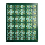
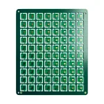
VII. Struktur & Merkmale: Vorteile der Panelisierung
Diese Leiterplatte nutzt Matrix-Panelisierung, wo mehrere einzelne Leiterplatten (z.B., 10×10 Array) sind auf einer größeren Produktionsplatte angeordnet, die durch verbunden ist Netze (Tabs).
Vorteile der Panelisierung:
- Produktionseffizienz: Mehrere Leiterplatten gleichzeitig hergestellt, Reduzierung der Rüstzeit der Maschine.
- Kostensenkung: Minimiert Ausschussmaterial und maximiert die Materialausnutzung.
- Einfache Montage: Bahnen können durch Routing oder getrennt werden V-Schnitt (V-Wertung) ohne einzelne Platinen zu beschädigen.
Zusätzliche Produktfunktionen:
- Hohe Zuverlässigkeit: FR-4 TG150 + ENIG/Hartgold hält rauen Umgebungen stand (hohe Temperatur, Luftfeuchtigkeit, Vibration).
- Niedrige Kosten: Ausgereifter 2-Schicht-Prozess ist 30%-50% billiger als Mehrschichtplatten.
- Anpassung: Unterstützt min. 0.1mm Lochgröße, min. 3mil Trace/Raum, und verschiedene Ausführungen (Eintauchen Silber, OSP, usw.).
- Umweltfreundlich: Konform mit RoHS Und ERREICHEN Standards; bleifreies Löten bereit für den weltweiten Export.
VIII. Herstellungsprozess: Strenge IPC-A-600 & IPC-6012-Steuerung
Der Arbeitsablauf von UGPCB wird strikt eingehalten IPC-A-600 (Qualitätsstandard) Und IPC-6012 (Leistungsspezifikation für starre Leiterplatten).
- Schneiden: Zuschneiden des FR-4-Laminats auf die erforderlichen Abmessungen (z.B., 18″x24″).
- Bohren: CNC-Bohren für Bauteillöcher (0.3mm) und Durchkontaktierungen (0.2mm).
- Chemisches Kupfer: Chemische Abscheidung von 1–2 μm Kupfer für die Verbindung zwischen den Schichten.
- Bildübertragung: Auftragen von Fotolack, entlarven, und Entwicklung zur Übertragung von Schaltkreismustern.
- Radierung: Entfernen von überschüssigem Kupfer, um endgültige Spuren zu bilden.
- Lötmaske: Beschichtung mit grüner Lötstopplackfarbe, entlarven, und Aushärten zum Schutz von Schaltkreisen.
- Oberflächenbeschaffung: ZUSTIMMEN (2u”) + Hartes Gold (30u”) Beschichtung für Lötbarkeit.
- Siebdruck: Drucken von Komponentenbezeichnern (R1, C2) und Logos.
- Elektrische Prüfung: Flying-Probe-Test um Kontinuität und Isolation zu prüfen (Keine Shorts/Öffnet).
- Fräsen/V-Schnitt: Einzelne Leiterplatten vom Panel trennen und Kanten anfasen.
- Endinspektion: AOI (Automatisierte optische Inspektion) für Kratzer, Oxidation, Maßhaltigkeit, und Zuverlässigkeitstests (Thermoschock, Vibration).
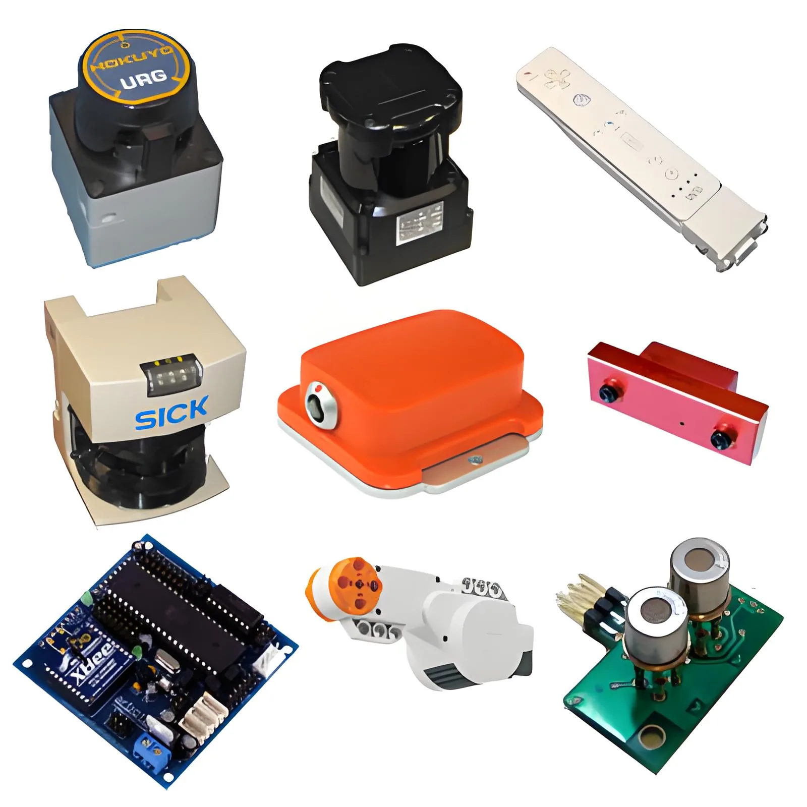
IX. Anwendungsszenarien
Dank seiner hohen Zuverlässigkeit und Wirtschaftlichkeit, Diese Leiterplatte wird häufig verwendet:
- Unterhaltungselektronik
- Mobiltelefone/Tablets: Ladetafeln, Leistungsmodule, Tastaturen.
- Wearables: Smartwatch-Motherboards, Fitness-Tracker-Sensoren.
- Haushaltsgeräte: AC-Steuerplatinen, Waschmaschinen-Displays.
- Industrielle Steuerung
- SPS-Module: I/O-Boards, Kommunikationsmodule.
- Sensoren: Signalverarbeitung für Temperatur-/Drucksensoren.
- Robotik: Servomotorsteuerung, Encoder-Schnittstellen.
- Kfz -Elektronik
- Infotainment: Navigation mainboards, Audiosteuerung.
- Sicherheitssysteme: Rückwärtsradarsteuerung, TPMS (Reifendrucküberwachung).
- Elektrofahrzeuge: Ladesäulenkontrolle, BMS (Batteriemanagementsystem) Hilfsplatinen.
- Medizinprodukte
- Tragbare Diagnose: Glukosemessgeräte, Blutdruckmessgeräte.
- Überwachung: EKG, Pulsoximeter-Signalplatinen.
- Chirurgisch: Steuerplatinen für minimalinvasive Instrumente.
- Andere Bereiche
- Telekommunikation: Router/Switch-Schnittstellenkarten.
- Luft- und Raumfahrt: Drohnen-Flugsteuerung, Satellitenkommunikation.
- Smart Home: Intelligente Schlösser, Intelligente Lichtsteuerung.
X. Warum wählen Sie UGPCB??
Als professioneller Leiterplattenhersteller mit über 10 jahrelange Erfahrung, UGPCB dient 1000+ Kunden weltweit.
- Fortschrittliche Ausrüstung: Japanische Mitsubishi-Bohrer, Deutsche LPKF-Belichtungsmaschinen, US-Testforschung Flying-Probe-Tester.
- Strenge Qualität: Zertifiziert mit ISO9001, ISO14001, und IATF16949 (Automobilindustrie).
- Schnelle Abwicklung: 24-Stunde Vorlaufzeit für Prototypen; 3-5 Tage für die Massenproduktion.
- Kostenlose Dienste: DFM (Design für die Fertigung) Überprüfen, kostenlose Angebote, und kostenlose Mustertests (für Erstbestellungen).
XI. Fordern Sie ein Angebot an: Beschleunigen Sie Ihre Time-to-Market
Wenn Sie brauchen 2-Lage starrer FR-4-Leiterplatten oder Fragen dazu haben ENIG+Hartgold oder Panelisierung, Kontaktieren Sie noch heute UGPCB!
- ✅ Kostenlose DFM-Rezension: Optimieren Sie Ihr Design, um Herstellungsfehler zu vermeiden.
- ✅ Kostenlose Mustertests: Überprüfen Sie die Leistung vor der Massenproduktion.
- ✅ Wettbewerbsfähige Preise: Kostengünstige Lösungen basierend auf Menge und Spezifikationen.
- ✅ Schnelle Lieferung: Prototypen in 24h, Massenproduktion in 3-5 Tage.
Zusammenfassung
UGPCB 2-Schichtstarre FR-4-Leiterplatte, mit FR-4 TG150 Grundmaterial Und ZUSTIMMEN + Oberfläche aus Hartgold, ist die erste Wahl für anspruchsvolle Anwendungen hohe Zuverlässigkeit Und niedrige Kosten. Egal, ob Sie ein Hersteller von Unterhaltungselektronik oder ein Automobilingenieur sind, Wir bieten maßgeschneiderte Lösungen, die alle Anforderungen erfüllen IPC-A-600-Standards.
Kontaktieren Sie uns jetzt, um Ihr Projekt zu starten und Marktchancen zu nutzen!


