

Descripción general del producto profesional: La alta velocidad de 12 capas, PCB de alta densidad
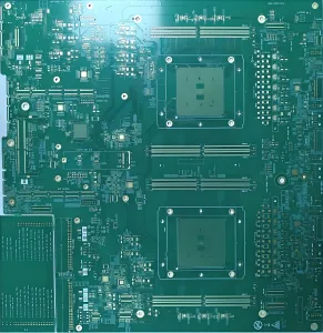
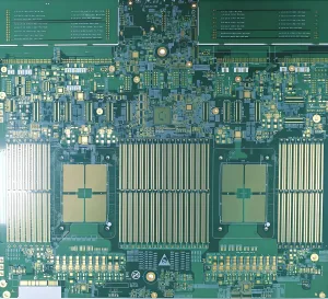
En la era de la transmisión de datos de alta velocidad y la integración de sistemas complejos, placas de circuito impreso convencionales (PCB) no cumplen con las demandas de rendimiento de la electrónica avanzada. El 12-capa de alta velocidad, PCB de alta densidad es la solución diseñada. Con hasta 12 capas conductoras alineadas con precisión, Permite interconexiones complejas y una transmisión de señal eficiente en un espacio compacto., sirviendo como el “sistema nervioso central” para equipos de redes de alta gama, servidores del centro de datos, informática de alto rendimiento (HPC), y hardware de IA.
Como experto fabricante de PCB y Proveedor de PCB, UGPCB aprovecha procesos avanzados para ofrecer servicios confiables 12-capa placa PCB producción, garantizar que sus productos mantengan una ventaja de rendimiento competitivo.
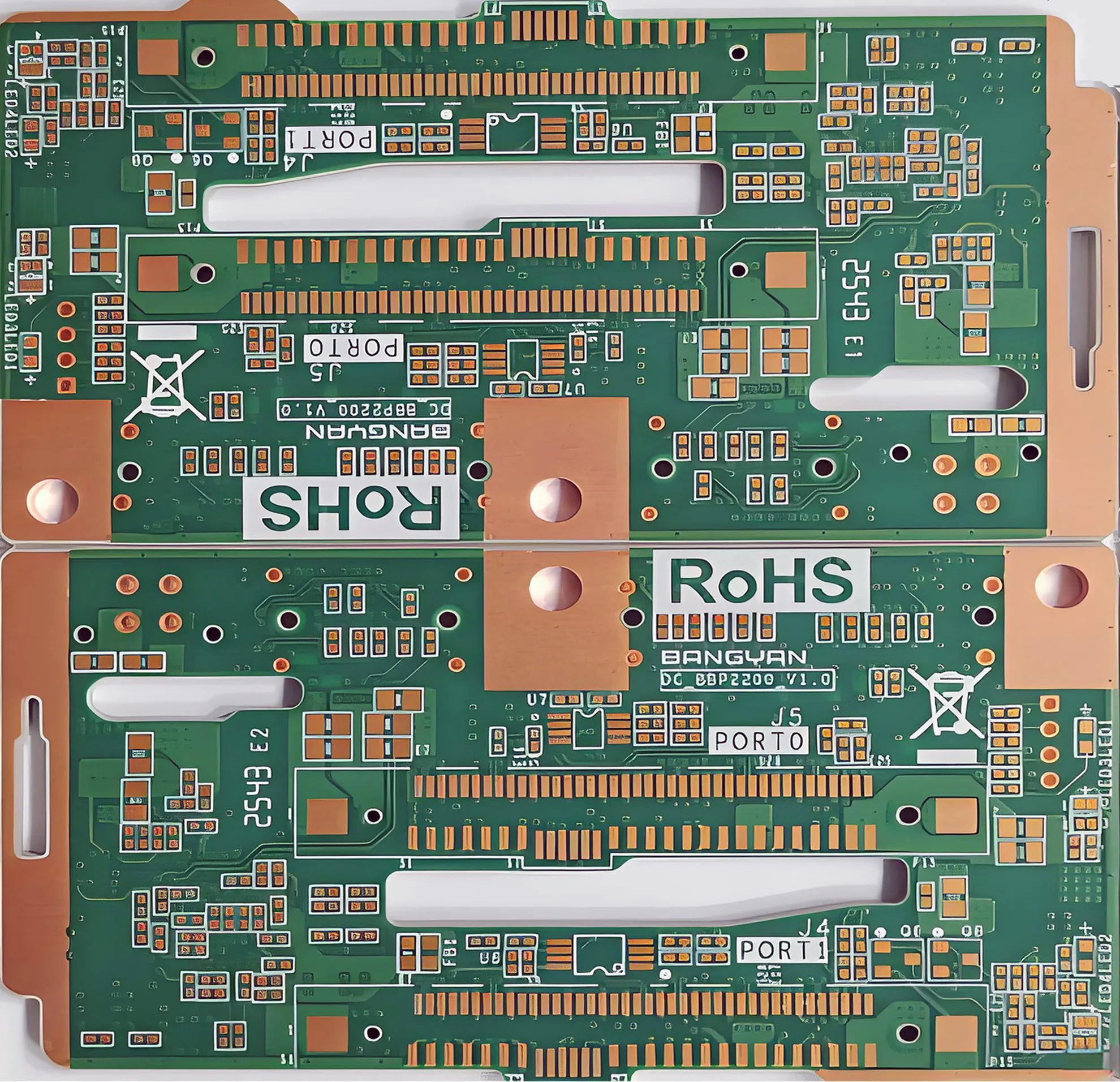
Análisis de parámetros en profundidad: La base del rendimiento
La capacidad de una alta calidad. placa de circuito impreso multicapa está definido por sus especificaciones. A continuación se muestra un análisis de los parámetros principales de este producto.:
-
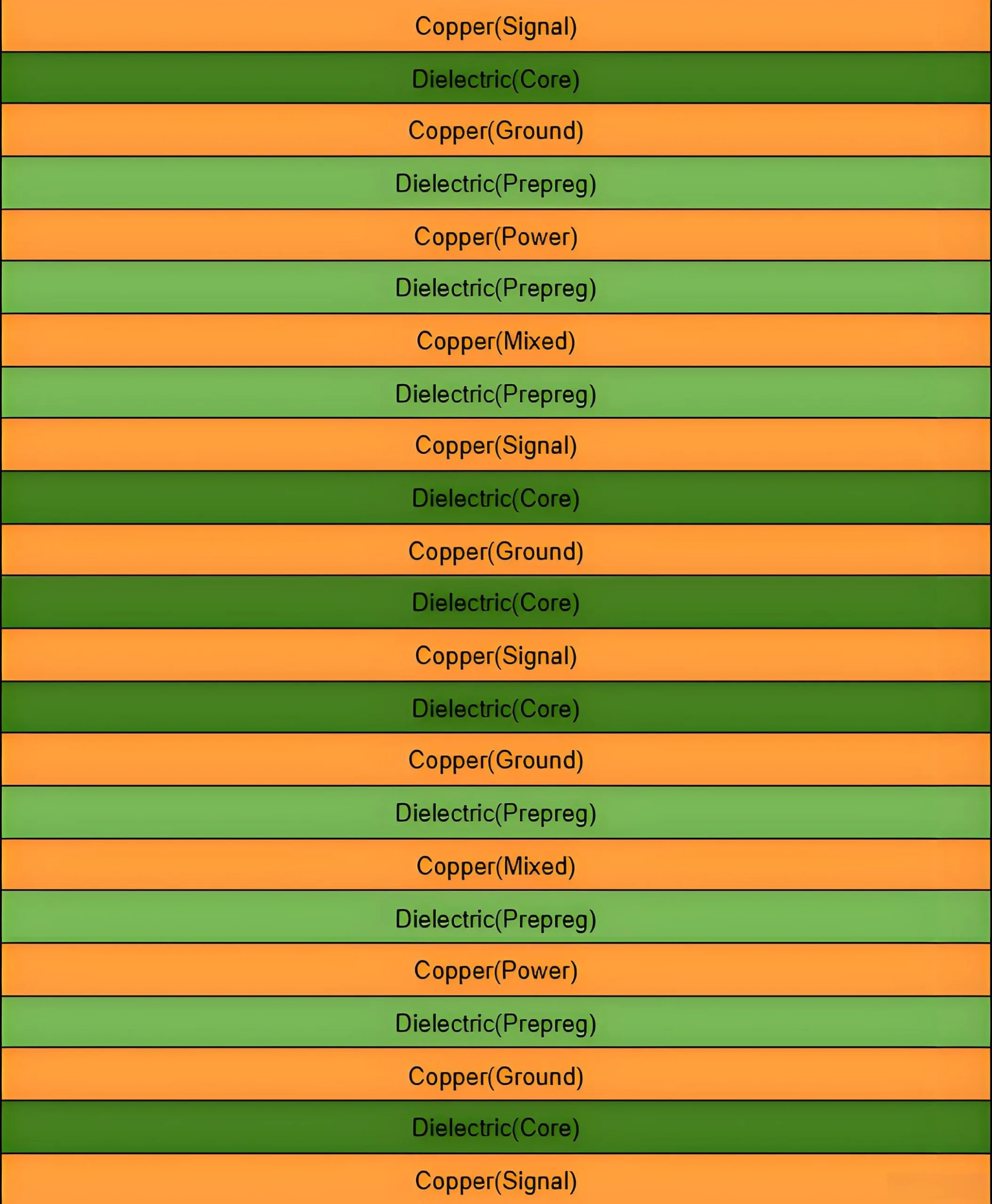
Recuento de capas & Acumulación: 12 capas. Este diseño de PCB multicapa ofrece una integridad de señal superior (Y), integridad del poder (PI), y rendimiento EMC en comparación con placas con menos capas. Permite planos de tierra y energía dedicados., proporcionando rutas de retorno claras para señales de alta velocidad.
-
Grosor del tablero & Tolerancia: 2.4mm ±10%. Este espesor robusto ofrece una excelente resistencia mecánica para placas posteriores y aplicaciones de factor de forma grande., Garantizar la confiabilidad durante el acoplamiento y la instalación.. La estrecha tolerancia garantiza la coherencia en el montaje..
-
Peso de cobre terminado: Distribución única:
1/1/1/1/1/2/2/1/1/1/1/1 oz. Esto indica que las capas internas (L6 & L7) utilizar 2 oz de cobre pesado, Diseñado específicamente para suministro de energía de alta corriente.. La capa exterior y otras capas de señal utilizan 1 oz de cobre., optimizado para grabado de líneas finas. Esta construcción híbrida es un sello distintivo de alta fiabilidad fabricación de PCB. -
Capacidades de procesos críticos:
-
Tamaño mínimo del orificio perforado: 0.2milímetros. Admite distribución BGA de alta densidad, mejorando la flexibilidad de enrutamiento.
-
Ancho/espacio mínimo de línea: 0.076milímetros / 0.09milímetros (3mil / 3.5mil). Logra Interconexión de alta densidad (IDH)-enrutamiento de nivel, esencial para la propagación de señales de alta velocidad.
-
-
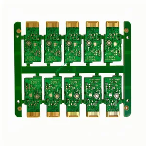
Acabado superficial: OSP (Conservante de soldabilidad orgánico). Compatible con soldadura con y sin plomo, Protege las almohadillas de cobre de la oxidación., Ofrece una excelente planitud de superficie., y es rentable: ideal para placas con SMT denso componentes.
Materiales núcleos & Tecnologías clave: Habilitación de una integridad de señal superior
-
Laminado de alto rendimiento: Utiliza Nanya NY6300S laminado de alta velocidad. Su alta temperatura de transición vítrea (tg >150°C) Garantiza estabilidad dimensional y confiabilidad durante la soldadura por reflujo a alta temperatura.. Su constante dieléctrica optimizada (Dk) y factor de disipación (df) Reduce significativamente la pérdida de señal en altas frecuencias., formando la base material para PCB de alta frecuencia.
-
Lámina de cobre avanzada: emplea rtf (Lámina con tratamiento inverso) cobre. Comparado con el estándar electrodepositado (Edición) frustrar, La lámina RTF presenta una textura más suave., superficie discreta en el lado tratado. Esto reduce la pérdida de señal debido a la “efecto piel” en altas frecuencias, mejorando críticamente el rendimiento de las señales diferenciales que exceden 10 GBPS.
-
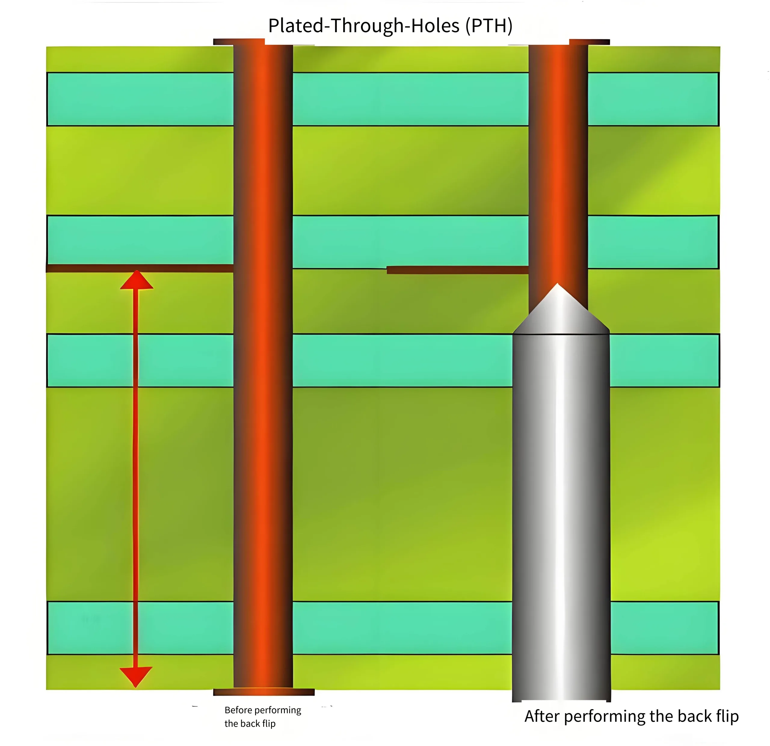
Proceso Crítico: Perforación de profundidad controlada (Perforación trasera): En 12 capas o más PCB multicapa, la porción no utilizada (talón) de una vía de orificio pasante puede causar una importante reflexión de la señal, integridad degradante. El proceso de perforación trasera elimina con precisión este no funcional a través de stub, eliminando su impacto negativo, una tecnología clave para PCB multicapa de alta velocidad actuación.
Flujo de producción & Seguro de calidad
UGPCB 12-proceso de fabricación de PCB en capas se adhiere estrictamente a Normas IPC e incluye Diseño para la fabricación (DFM) revisar, imágenes de la capa interna, laminación, perforación (incluyendo perforación trasera), enchapado, imágenes de la capa exterior, aplicación de máscara de soldadura, acabado superficial (OSP), enrutamiento, pruebas electricas, e inspección final. Cada etapa está respaldada por equipos de medición de precisión. (AOI, Prueba de impedancia, Prueba de sonda voladora), asegurando cada tarjeta de circuitos entregado cumple con las especificaciones de diseño y nuestros estándares de alta calidad.
Aplicaciones típicas & Clasificación de productos
Este alto rendimiento placa PCB está diseñado para entornos eléctricos exigentes y sistemas complejos, utilizado principalmente en:
-
Red de alta gama & Equipo de comunicación: Placas base centrales para módulos ópticos 400G/800G, enrutadores de alta gama, y cambia.
-
Centro de datos & Computación en la nube: Placas base de servidor, tarjetas aceleradoras, placas posteriores de almacenamiento.
-
Informática de alto rendimiento: Placas base para estaciones de trabajo, Tarjetas informáticas GPU, Hardware acelerador de IA.
-
Prueba avanzada & Instrumentos de medición: Tarjetas internas para instrumentos que procesan señales de muy alta frecuencia..
Clasificación científica de productos:
-
Por recuento de capas: PCB multicapa (>8 capas)
-
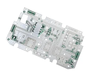
Por tipo de tecnología: PCB de alta velocidad/alta frecuencia, PCB HDI, PCB de cobre pesado (parcial)
-
Por aplicación: PCB de infraestructura de telecomunicaciones, PCB de centro de datos/servidor
¿Por qué elegir UGPCB para su PCB de alta velocidad de 12 capas??
-
Experiencia técnica: Dominio demostrado de perforación trasera y Lámina de cobre RTF Aplicación para abordar desafíos de diseño de alta velocidad..
-
Fabricación de precisión: Capaz de 3/3.5 mil línea/espacio, cumplir con estrictos requisitos de interconexión de alta densidad.
-
Integridad de materiales: Uso principal de productos de buena reputación. laminados de alta velocidad como Nanya NY6300S garantiza un rendimiento fundamental.
-
Soporte de diseño: Experto diseño de PCB y revisión de DFM Servicios para eliminar riesgos de su proyecto desde el principio..
-
Calidad constante: Un totalmente controlado producción de PCB y el sistema de inspección ofrece productos confiables en los que puede confiar.
Listo para elevar su hardware? Póngase en contacto con los ingenieros de UGPCB para obtener una cotización gratuita de PCB y Análisis DFM en su próximo proyecto de tablero de alta velocidad de 12 capas.






Este sitio web de Internet podría ser un recorrido por la información que deseaba al respecto y no sabía quién debería hacerlo.. Vislumbra aquí, y lo descubrirás por completo.