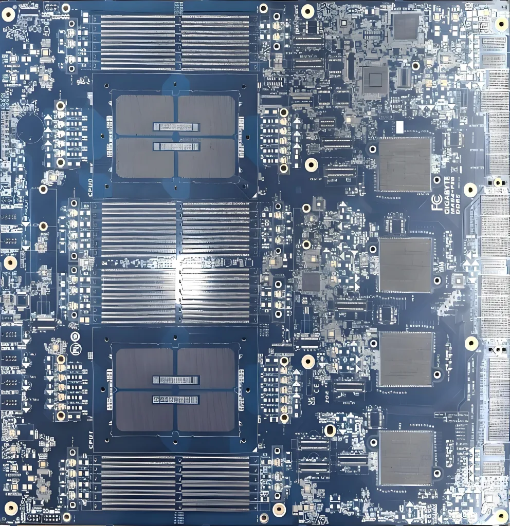
UGPCB 26-Layer High-Performance Server PCB: The Core Foundation for Data Center Computing Power
In the digital era, servers are the “super-brains” processing massive data, y el servidor tarjeta de circuito impreso (placa de circuito impreso) is the critical “red neuronal” of this brain. A well-designed, precisely manufactured high-end server motherboard PCB directly determines a data center’s processing speed, power efficiency, and long-term operational stability. Leveraging deep expertise in de alta velocidad, con cuenta de alta capa fabricación de PCB, UGPCB has developed this flagship 26-layer server PCB for next-generation High-Performance Computing (HPC), Servidores AI, and cloud data centers. It is engineered to deliver exceptional electrical performance and reliable physical structure to support extreme computational loads.
Definición del producto & Descripción general: What is a High-End Server PCB?
A high-end server PCB is a complex, multi-layer circuit board designed to host core components like CPUs, memoria, high-speed interfaces (p.ej., Pítico, CXL), and power management units, and to establish ultra-high-speed, highly reliable electrical connections between them. It is not just a mechanical substrate but a critical platform for ensuring signal integrity and power integrity at GHz frequencies. Este UGPCB product features a sophisticated 26-layer PCB stack-up, utilizing advanced materials and processes specifically engineered for demanding applications like big data processing and AI training.
Core Design Points & Principio de trabajo
The primary function of a server PCB is to provide a low-loss, low-interference transmission path for high-speed digital signals and high-current power delivery. Its design revolves around several key principles:
-
Integridad de señal (Y): The use of materiales de alta velocidad (tg 170) and precise control over trace width/spacing of 0.08mm/0.09mm minimizes signal attenuation and distortion, ensuring error-free data transmission at rates of tens of Gb/s.
-
Integridad de poder (PI): The incorporation of 2oz heavy copper (2/2 onz) for power and internal planes reduces DC resistance and temperature rise, delivering ample and clean power to high-power chips like CPUs/GPUs.
-
Control de impedancia & Fondos de fondo: Strict impedance control is applied to high-speed channels. A key innovation is the use of backdrilling technology to remove the unused conductive stub (barrel) of plated through-holes, eliminating signal reflection points—a core process for enhancing signal quality in PCB de alta velocidad.
-
Gestión Térmica & Fiabilidad: A finished board thickness of 2.97mm ±10% y high Tg 170 material provide excellent mechanical strength and heat resistance, ensuring the PCB remains stable and reliable under the prolonged, high-temperature, full-load operation of servers.
Especificaciones técnicas & Materiales
-
Recuento de capas & Espesor: 26 capas, finished board thickness 2.97mm ±10%.
-
Copper Weight Stack-up: Complex configuration: 1/1/H/1/H/1/H/1/H/1/H/2//2/2/H/1/H/1/H/1/H/1/H/1/1 oz. Critical power layers use 2oz heavy copper to balance signal and power needs.
-
Material central: Taiyao TU883 de alta velocidad, low-loss laminate con un Temperatura de transición vítrea (tg) of 170°C. It offers a very low dielectric constant (Dk) and dissipation factor (df), making it a top-tier choice for high-speed PCB materials.
-
Line Precision: Minimum trace width/space of 0.08milímetros / 0.09milímetros, enabling high-density routing.
-
Micro-Via Technology: Supports a minimum mechanical drill diameter of 0.20mm, meeting high-density interconnection (IDH) requisitos.
-
Acabado superficial: Conservante de soldabilidad orgánico (OSP) provides a flat, highly solderable surface for high-performance BGA and chip componentes, offering excellent cost-effectiveness.
Product Classification, Estructura & Características
-
Scientific Classification: This product belongs to the category of “High-End Multi-Layer High-Speed Server Motherboard PCBs”, específicamente “Tg alta, High-Layer-Count, Con pleno recortado, Heavy-Copper Power Delivery PCBs”.
-
Core Structural Features:
-
Multi-Layer Lamination: Precise arrangement of signal, suelo, and power planes creates effective electromagnetic shielding and low-impedance return paths.
-
Backdrill Structure: Through-holes for critical high-speed links (p.ej., PCIe lanes, memory slot connections) are backdrilled to significantly enhance high-frequency performance.
-
RTF Copper Foil Application: The use of Reverse Treated Foil provides a smoother copper surface, further reducing signal loss during transmission along the conductor.
-
Rigorous Production Process
UGPCB’s manufacturing process strictly adheres to IPC-A-600G/6012 Class 2/3 estándares, with enhanced controls for server PCBs:
Material Cutting → Inner Layer Imaging & AOI Inspection → Lamination & Drilling → Electroless & Electrolytic Copper Deposition → Backdrilling Process → Outer Layer Imaging → Secondary AOI & Impedance Testing → Solder Mask & OSP Application → Electrical Test (Flying Probe/Test Fixture) → Final Visual Inspection & Embalaje.
Entre estos, backdrilling y prueba de impedancia are critical control points ensuring the quality of this high-performance server PCB.
Target Applications
This product is specifically designed and manufactured for the following high-end applications:
-
Inteligencia artificial & Machine Learning Servers: Hosting training and inference GPU/ASIC clusters.
-
Computación en la nube & Data Center Servers: For High-Performance Computing (HPC) clusters and virtualization hosts.
-
Enterprise Storage Servers: Storage devices requiring high reliability and numerous high-speed data interfaces.
-
5G Core Network Equipment: Network infrastructure handling high-speed data switching.