
When digital and RF systems push beyond multiple GHz, conventional Materiales de PCB hit bottlenecks in signal integrity, estabilidad térmica, y control de impedancia. UGPCB’s communication high frequency hybrid PCB solves these challenges.
1. Descripción general del producto
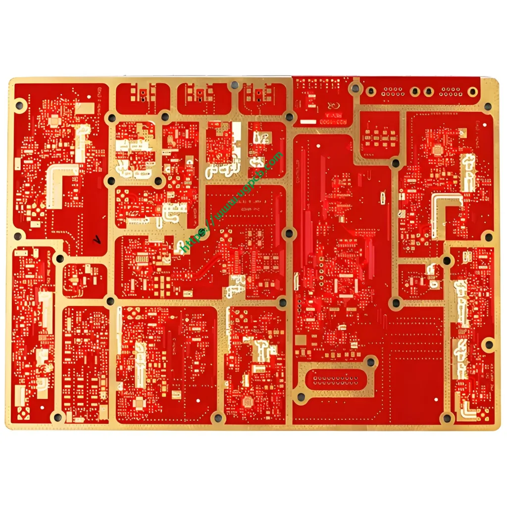
Nombre del producto: UGPCB 6‑Layer Communication High Frequency Hybrid PCB
Modelo: UG‑HYBRID‑6L‑RF01
Especificaciones clave: 6 capas / Ro4350B+FR4 mixed dielectric / 1.6mm de espesor del tablero / 210mm × 280mm size / Acabado superficial ENIG / minimum mechanical drilled hole 0.25mm
Positioning: A cost‑effective interconnect solution for RF front‑ends and high‑speed digital mixed circuits. By placing Rogers RO4350B high‑frequency laminate on the top RF signal layers and FR‑4 on the bottom power/ground and low‑speed digital layers, this design balances signal integrity, estabilidad térmica, y costo de fabricación.

2. Definition – What is a High Frequency Hybrid PCB?
A high frequency hybrid PCB (also called mixed dielectric multilayer board) uses two or more materials with different dielectric properties in one multilayer printed circuit board.
This 6‑layer hybrid PCB has the following stackup:
| Capa | Función | Material | Parámetro clave |
|---|---|---|---|
| L1 | RF signal | RO4350B (0.2milímetros) | Dk=3.48±0.05@10GHz, Df=0.0037 |
| L2 | RF ground | RO4350B | Low‑loss reference plane |
| L3 | High‑speed digital | RO4450™ bondply + FR‑4 | Transition, coincidencia de impedancia |
| L4 | Power plane | FR‑4 | Tg alta, bajo costo |
| L5 | Digital signal | FR‑4 | Standard epoxy glass |
| L6 | Digital ground | FR‑4 | Mechanical support and heat dissipation |
“Mixed dielectric construction significantly reduces cost – using high‑frequency material only on the layers that carry RF signals, and FR‑4 for the rest.”
3. Pautas de diseño
3.1 Critical Material Parameters
This product uses Rogers RO4350B (ceramic‑filled hydrocarbon laminate) and FR‑4. Key RO4350B specifications (source: Rogers data sheet):
| Parámetro | Valor típico | Condición de prueba | Reference |
|---|---|---|---|
| Process Dk | 3.48±0,05 | 10GHz | IPC‑TM‑650 2.5.5.5 |
| Design Dk | 3.66 | 10GHz | Copper roughness correction |
| factor de disipación (df) | 0.0037 | 10GHz | Low‑loss RF applications |
| Z‑axis CTE | 32 PPM/℃ | -55℃ to 288℃ | Matches copper (17 PPM/℃) |
| Conductividad térmica | 0.69 W/m·K | 50℃, ASTM D5470 | Better than FR‑4 |
| Inflamabilidad | UL 94 V‑0 | UL standard | For active and high‑power RF |
fuente de datos: Rogers Corporation RO4350B™ Laminate Data Sheet
3.2 Control de impedancia
Impedance control on a 6‑layer hybrid PCB is challenging because of the Dk discontinuity. Use a 3D electromagnetic solver and apply a copper roughness correction factor (typically 1.2–1.5). According to IPC‑2141A, characteristic impedance tolerance for RF PCBs should be within ±7%. UGPCB achieves ±5%.
3.3 Laminate Stackup Design (Total thickness 1.6mm)
- Arriba (L1‑L2): RO4350B 0.2mm × 2 = 0.4mm
- Middle (L3): RO4450™ prepreg 0.1mm + FR‑4 core 0.6mm = 0.7mm
- Bottom (L4‑L6): FR‑4 core + prepreg = 0.5mm
- Total: 1.6milímetros
Use a dynamic pressure curve during lamination to manage stress from CTE mismatch between RO4350B and FR‑4.
4. Principio de trabajo
Integridad de la señal: Dielectric loss dominates high‑frequency loss. The medium attenuation constant is:
Dónde:
- = dielectric attenuation constant
- = Permitividad relativa (design value)
- = free‑space wavelength
- = dissipation factor (df)
RO4350B has Df = 0.0037 VS. FR‑4’s 0.020. That reduces dielectric loss by about 80%, ensuring low‑loss transmission up to 30GHz.
Thermal‑mechanical stability: RO4350B’s Z‑axis CTE of 32 ppm/℃ matches copper (17 PPM/℃) far better than FR‑4 (50–70 ppm/℃). This improves plated through‑hole (PTH) reliability under thermal cycling. Tested per IPC‑TM‑650 2.6.7, the board survives 1000 cycles from -55℃ to 125℃ without delamination.
5. Aplicaciones primarias
UGPCB’s 6‑layer communication high frequency hybrid PCB serves five major areas:
5.1 5G Communication Base Stations (AAU/RRU)
- Frequency bands: 28GHz and 39GHz millimeter wave
- Requisito: Insertion loss < 0.31 dB/cm@40GHz, power handling >200 W/m²@38GHz
- Advantage: Hybrid construction cuts material cost by 30–40% vs. all‑high‑frequency material

5.2 77GHz/79GHz Automotive Radar
- Use cases: Autonomous driving 4D imaging radar, blind spot detection, control de crucero adaptativo
- Requisito: Range error <0.25m from -40℃ to 125℃, azimuth resolution 0.08°
- Actuación: IMS 2025 report shows phase consistency of ±0.8° over full temperature range for 77GHz hybrid radar modules
5.3 Satellite Communication Payloads (Ka‑band)
- Frequency range: 17.7 - 31 GHz
- Advantage: 45% weight reduction vs. ceramic substrates while maintaining >85% efficiency
5.4 Fiber‑to‑the‑Home (FTTH) Equipo
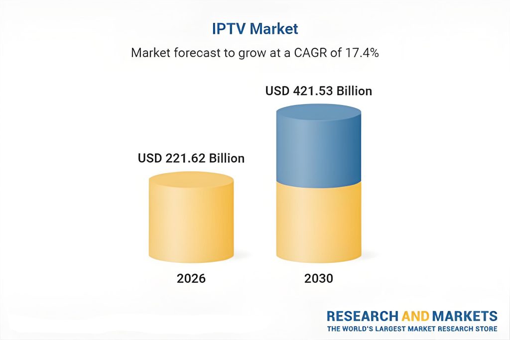
- Market trend: Global IPTV market from $189.25B (2025) to $421.53B (2030), Tocón 17.4%
- Impacto: High‑bandwidth, low‑latency PCBs are essential
5.5 High‑Speed Digital Mixed‑Signal Systems
- Fields: Medical imaging, industrial high‑frequency inspection, military communication terminals
- Requisito: Coexist 10+ Gbps digital signals with GHz‑range RF signals
6. Clasificación científica (per IPC‑2221)
| Classification Dimension | Categoría | Basis |
|---|---|---|
| Material system | Mixed dielectric PCB | RO4350B + FR‑4 |
| Frequency characteristic | RF / PCB de microondas | Up to 30GHz |
| Layer count | 6‑layer multilayer board | 6 conductive layers |
| Technical difficulty | HDI hybrid lamination | Non‑expansion material matching |
| Solicitud | Communication RF PCB | infraestructura de telecomunicaciones |
| IPC performance class | IPC‑6012 Class 3 | High‑reliability equipment |
7. Materials in Detail
7.1 RO4350B High‑Frequency Laminate
- Glass‑reinforced hydrocarbon + ceramic filler
- Dk: 3.48±0.05@10GHz, temperature coefficient ~ -50 PPM/℃ (-50℃ to +150℃)
- df: 0.0037@10ghz
- Z‑axis CTE: 32 ppm/℃ – matches copper for PTH reliability
- Conductividad térmica: 0.69 W/m·K (VS. FR‑4 0.25–0.35)
- UL 94 V‑0 – suitable for active and high‑power RF designs
- Process compatibility: Same FR‑4 processing; no special pre‑treatment needed (unlike PTFE)
7.2 FR‑4 Epoxy Glass Laminate
- Woven glass fabric + resina epoxídica
- Dk: 4.2–4,8 (1MHz–1GHz), df: 0.020–0,025
- Costo: 1/5 a 1/10 of RO4350B
7.3 RO4450™ High‑Frequency Bondply
- Bonding layer between RO4350B and FR‑4
- Dk: 3.52±0.05@10GHz (gradient transition)
- df: 0.0040@10ghz
7.4 Acabado superficial ENIG (Oro de inmersión de níquel químico)
- Espesor del níquel: 3–6μm (IPC‑4552 Class 2)
- Espesor del oro: 0.05–0.10μm
- Ventajas: Solderability, flatness, oxidation resistance, fine‑pitch BGA assembly
- Estándar: IPC‑4552
8. Especificaciones de rendimiento
8.1 Rendimiento eléctrico
| Parámetro | Valor | Test Method |
|---|---|---|
| Characteristic impedance (RF layers) | 50Ω ±5% (personalizable) | IPC‑2141A |
| Dk (RF layers @10GHz) | 3.48±0,05 | IPC‑TM‑650 2.5.5.5 |
| Insertion loss | 0.31 dB/cm @40GHz | Microstrip line VNA |
| Dielectric strength | ≥40 kV/mm | IPC‑TM‑650 2.5.6 |
| Resistencia de aislamiento | >10⁹ Ω (normal condition) | IPC‑TM‑650 2.5.17 |
| Withstanding voltage | 1000 VCC, 60s no breakdown | IPC‑TM‑650 2.5.7 |
8.2 Mechanical Performance
| Parámetro | Valor | Test Method |
|---|---|---|
| Tolerancia de espesor | ± 10% | IPC‑6012 |
| Dimensional stability | <0.3 mm/m | IPC‑TM‑650 2.2.4 |
| Fuerza de pelado (1onzas de cobre) | ≥1.0 N/mm | IPC‑TM‑650 2.4.8 |
| Flexural strength | ≥350 MPa | IPC‑TM‑650 2.4.4 |
| Pad pull‑off force | ≥5.0 kg/cm² | IPC‑TM‑650 2.4.21 |
8.3 Rendimiento térmico
| Parámetro | Valor | Test Method |
|---|---|---|
| tg (FR‑4 area) | ≥150℃ (TG150) | IPC‑TM‑650 2.4.25 |
| Thermal stress | 288℃, 10s × 5 ciclos | IPC‑TM‑650 2.4.13 |
| Ciclismo térmico | -55℃ ↔ 125℃, 1000 ciclos, Sin delaminación | IPC‑TM‑650 2.6.7 |
| Lead‑free reflow | 260℃, 5 ciclos | IPC/JEDEC J‑STD‑020 |
| Moisture sensitivity level | MSL 1 | IPC/JEDEC J‑STD‑020 |
8.4 Reliability Certifications
- IPC‑6012 Class 3 – high‑reliability equipment
- IPC‑6018B – qualification for high‑frequency (microonda) PCB
- UL 94 V‑0
- MIL‑PRF‑31032 - 1000 thermal cycles from -55℃ to 125℃
100% flying probe electrical test + AOI. End‑product meets IPC‑A‑600 Class 3.
9. Características estructurales
Asymmetric 6‑layer hybrid build:
- L1‑L2 (RO4350B): RF front‑end (Pensilvania, LNA, filtros) – signal integrity critical zone
- L3 (transición): Impedance matching and signal layer change – isolates RF from high‑speed digital
- L4‑L6 (FR‑4): Power management, digital control, mechanical support – low‑cost conventional circuits
ENIG finish: Flat surface ensures consistent impedance control. Supports BGA, QFN, fine‑pitch packages. Gold layer protects copper and guarantees solderability after long storage.
Perforación de precisión & PTH: Minimum mechanical hole diameter 0.25mm (HDI microvias down to 0.1mm available). Hole copper thickness ≥20μm (Clase IPC 3). Plasma treatment with different gas mixtures for RO4350B and FR‑4 layers.
10. Flujo del proceso de fabricación
18 key steps:
① IQC → ② Inner layer imaging (RF and digital separately) → ③ Brown oxide → ④ Pre‑lamination plasma activation → ⑤ Hybrid lay‑up → ⑥ High‑pressure lamination (dynamic pressure curve) → ⑦ X‑ray target drilling → ⑧ Mechanical drilling (0.25mm min) → ⑨ Plasma desmear (dual cycle) → ⑩ Electroless copper → ⑪ Outer layer imaging → ⑫ Pattern plating (cobre + tin) → ⑬ Outer layer etching (tin strip) → ⑭ AOI → ⑮ Solder mask → ⑯ ENIG → ⑰ Electrical test → ⑱ Final inspection/packaging
Critical process details:
- Pre‑lamination plasma (step 4): CF₄‑N₂‑O₂ for FR‑4; helium (He) for RO4350B
- Lamination curve (step 6): Dynamic pressure – FR‑4 cures first (~180℃), then pressure and temperature rise to >200℃ for RO4350B
- Perforación (step 8): Step feed and tool life management handle hardness difference
- desmechar & PTH (steps 9‑10): Dual‑cycle process due to different chemical behaviors; hole copper ≥20μm
11. Competitive Advantages
Cost‑performance balance: All‑RO4350B 6‑layer material costs >$200/m². Hybrid uses RO4350B only on 25% of thickness →30‑40% material cost reduction.
Fiabilidad: RO4350B Z‑axis CTE = 32 ppm/℃ matches copper (17 PPM/℃). Full FR‑4 has 50‑70 ppm/℃. Hybrid reduces PTH stress. Passes 1000 cycles -55℃ to 125℃ (IPC‑TM‑650 2.6.7).
Dimensional stability: Low CTE reduces warpage, improves SMT yield.
| Direction | RO4350B CTE | FR‑4 CTE (típico) |
|---|---|---|
| X‑axis | 10 PPM/℃ | 14 PPM/℃ |
| Y‑axis | 12 PPM/℃ | 16 PPM/℃ |
| Z‑axis | 32 PPM/℃ | 50‑70 ppm/℃ |
Vs. full PTFE (p.ej., Rogers RT/Duroid):
| Característica | RO4350B+FR‑4 hybrid | Full PTFE |
|---|---|---|
| Process compatibility | Standard FR‑4 line | Special equipment & treatment |
| metalización de PTH | Estándar | Sodium naphthalene or plasma |
| Dimensional stability | Excelente (glass reinforced) | Poor, flows |
| Costo | 30‑50% lower | Alto |
12. Resumen & Inquiry Guidance
UGPCB’s 6‑layer communication high frequency hybrid PCB is the ideal interconnect for RF/digital mixed signal systems. It serves 5G base stations, satellite Ka‑band payloads, 77GHz automotive radar, and high‑speed digital applications. By placing RO4350B only on the critical RF layers, we achieve optimal performance at a significantly lower cost.
Key data recap:
✅ Dk = 3.48 ± 0.05 @10ghz (Rogers official)
✅ Df = 0.0037 @10ghz
✅ Z‑axis CTE = 32 PPM/℃ (matches copper)
✅ Insertion loss ≤ 0.31 dB/cm @40GHz (IPC‑6018B verified)
✅30‑40% material cost reduction VS. all‑high‑frequency material
✅ Passes 1000 thermal cycles -55℃ ↔ 125℃
Limited‑time prototyping offer
📩 Get your custom quote and technical proposal
UGPCB offers a 7‑working‑day quick‑turn service for 4‑ to 10‑layer hybrid PCBs. We provide free DFM analysis.
👉 Send your Gerber files and stackup design to our technical support email. We will reply with a technical assessment and precise quote within 4 horas.
UGPCB – Your trusted hybrid high‑frequency PCB manufacturer. From prototype to volume production, we deliver one‑stop 6‑layer mixed dielectric solutions to accelerate your 5G and millimeter‑wave radar products.
*Data sources: Rogers Corporation RO4350B™ Data Sheet, IPC‑6012D/6018B standards, IPC‑TM‑650 test methods, GSMA 2026 telecom outlook, IMS 2025 International Microwave Symposium technical report.*


