
Double-Sided Power PCBs: Confiable, High-Current Boards for Demanding Applications
In an era of high-power electronics, stable and efficient power management is critical. A placa de circuito impreso (tarjeta de circuito impreso) optimized for power transmission and conversion is often the cornerstone of system reliability. Our double-sided power PCBs are engineered to meet the stringent challenges of high current, voltage, y gestión térmica.
Descripción general del producto: What is a Double-Sided Power PCB?
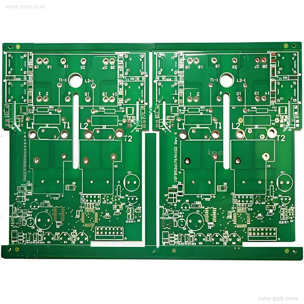
A double-sided power PCB is a specialized printed circuit board designed to carry and distribute high current and manage substantial power across its two layers. Unlike standard signal PCBs, its core design objectives are low impedance, high current-carrying capacity, and superior thermal performance. We use FR-4 (a flame-retardant glass-reinforced epoxy laminate) as the base material, ensuring every board performs reliably in applications like power converters, unidades de motor, and industrial power supplies through stringent process control.
Especificaciones principales
-
Modelo: Double-Sided Power PCB
-
Materia prima: High-Quality FR-4
-
Recuento de capas: 2 capas
-
Grosor del tablero: 1.6milímetros (Estándar, excellent mechanical strength)
-
Espesor de cobre (Finished): 1onz (35µm) - A key parameter for current carrying capacity. (2onz, 3oz available)
-
Acabado superficial: HASL sin plomo (Nivelación de soldadura por aire caliente). Provides excellent solderability and cost-effectiveness.
-
mín.. Traza/Espacio: 6mil (0.15milímetros), sufficient for most power layouts.
-
Solder Mask Color: Verde (Estándar)
Design Essentials & Principio de trabajo
Key Design Considerations:
-
Wide Traces & Cobre pesado: Power paths (p.ej., Vin, Vout, Gnd) use the widest possible traces with 1oz or thicker copper to minimize resistance, heat generation, and voltage drop.
-
Adequate Via Stitching: Multiple vias in arrays are used to connect the same power net on both layers, significantly reducing parasitic resistance and inductance of the vias and enhancing current capacity.
-
Gestión Térmica: Strategic placement of heat-generating components (p.ej., MOSFET, inductores) alongside thermal vias y exposed copper pads to efficiently transfer heat to the opposite side or an external heatsink.
-
Safety Spacing: Electrical clearance and creepage distances for high-voltage lines are strictly set according to safety standards (p.ej., UL, CEI) to ensure operational safety.
Principio de trabajo:
The double-sided power PCB serves as a passive interconnection platform. Its function is to provide optimal electrical and physical connections for active power componentes (circuitos integrados, transformers, condensadores, inductores). Through meticulously designed high-power traces, it ensures energy is transferred from input to conversion circuitry and then to the load with minimal loss and heat generation. Effective thermal path design keeps component junction temperatures within safe limits, enabling reliable Asamblea de PCBA and long-term stable operation.
Product Categories, Materiales & Características estructurales
Common Applications/Categories:
-
DC-DC Converter PCBs
-
AC-DC Power Supply Module PCBs
-
Motor Driver PCBs
-
Inverter/VFD PCBs
-
High-Power LED Driver PCBs
-
Sistema de gestión de batería (Bms) PCB
Materiales utilizados:
-
sustrato: FR-4, offering excellent insulation, resistencia mecánica, y retardante de llama (94V-0).
-
Conductive Layer: Electro-deposited copper foil (starting at 1oz, customizable to 2oz, 3onz, and beyond).
-
Máscara de soldadura: Standard green LPI (Liquid Photo-Imageable) ink for protection.
-
Acabado superficial: Standard Lead-Free HASL. Other finishes like ENIG or OSP are available upon request.
Características estructurales:
-
Dual-Side Layout: Components can be placed on both top and bottom layers, maximizing space for efficient power routing.
-
Reinforced Power Planes: While not having dedicated power planes, large copper pours on both layers create highly effective “pseudo” power planes.
-
Integrated Thermal Management: Features like thermal vias and large exposed copper areas facilitate heat dissipation to enclosures or heatsinks.
-
Robust Construction: The standard 1.6mm board thickness provides superior mechanical rigidity, suitable for heavy components like large capacitors and heatsinks.
UGPCB Standard Production Flow & Performance Advantages
Our Manufacturing Process:
DFM Review → Material Prep → Drilling → Plating (PTH) → Pattern Transfer → Pattern Plating (Copper Build-up) → Etching → Solder Mask Application → Surface Finish (HASL) → Silkscreen → Electrical Testing → Final Inspection → Packaging & Shipping
We maintain strict control over every step, particularly copper plating thickness and etch uniformity, to ensure precision and current-carrying capability of power traces.
Key Performance Advantages:
-
High Current Capacity: Optimized copper weight and trace design for handling Ampere-level currents.
-
Low Thermal Resistance: Innovative cooling features effectively reduce hot spot temperatures, extending component lifespan.
-
High Stability: Rigorous process and material control ensure stable performance in harsh environments (high temp/humidity).
-
Strong Compatibility: Proven HASL surface finish offers excellent solderability for volume tarjeta de circuito impreso producción.
-
Cost-Effective: Provides competitive pricing for both PCB quick-turn prototypes and volume production without comp
Wide Range of Applications
UGPCB’s double-sided power PCBs are the ideal choice for numerous high-power electronic devices:
-
Controles Industriales: Variable Frequency Drives (VFDs), servo drives, PLC power modules.
-
Nueva energía: PV inverters, Energy Storage System (ESS) power conversion systems, charging pile modules.
-
Electrónica automotriz: Cargadores a bordo (OBC), Convertidores DC-DC, motor controllers.
-
Electrónica de Consumo: High-wattage adapters, gaming console PSUs, high-end audio amplifiers.
-
Telecom Equipment: Base station power supplies, network equipment power distribution boards.
Why Choose UGPCB for Your Double-Sided Power PCBs?
We understand the complexities of power diseño de PCB. Choosing UGPCB means gaining more than just a circuit board; you gain a reliable power solution partner. We offer comprehensive support from PCB design review y quick-turn prototyping to volume production, ensuring your product’s smooth journey from concept to market.
Contact a UGPCB sales engineer today for a customized quote and technical solution for your double-sided power PCB needs! Let our expertise empower your product with stable, reliable performance.


