

1. Descripción general del producto
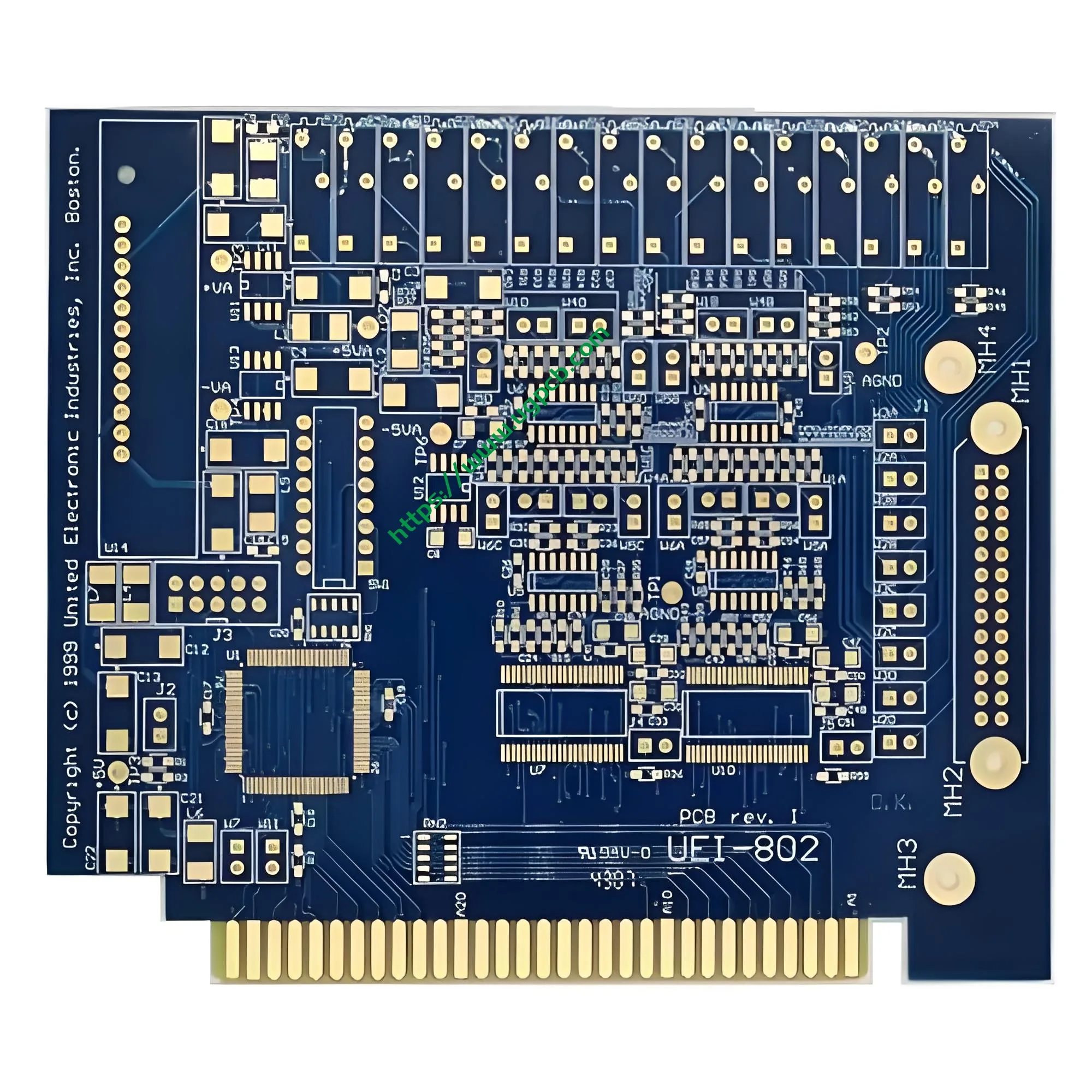
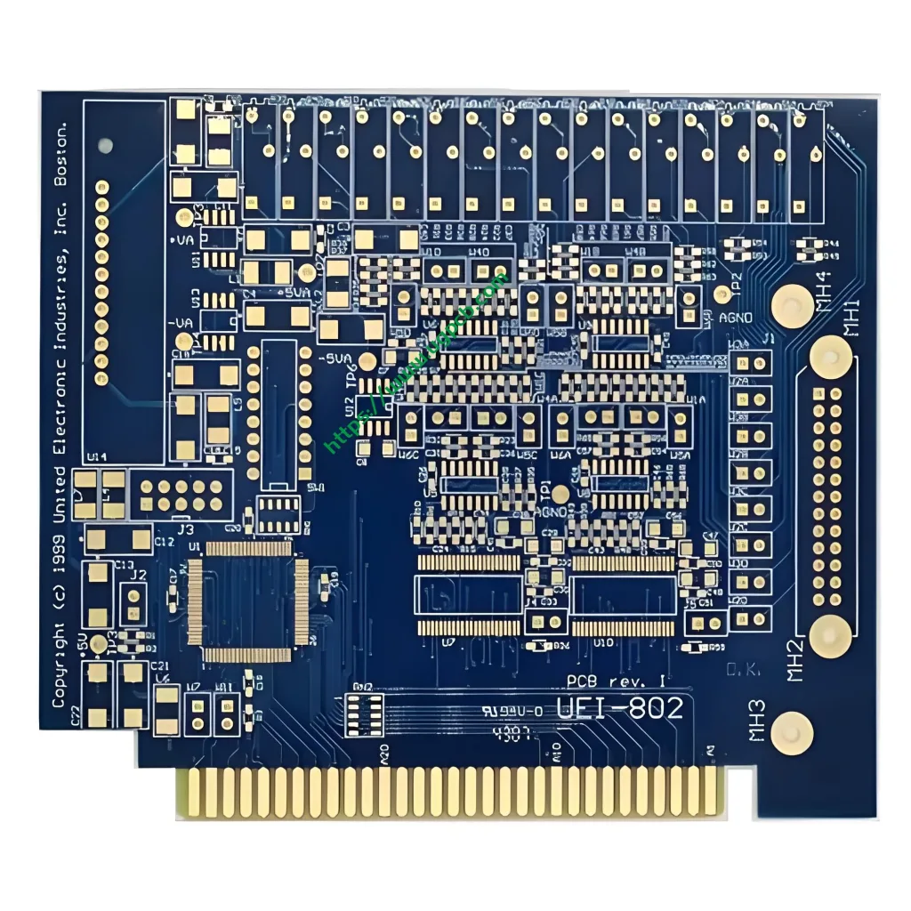
Un dedo de oro de doble cara placa de circuito impreso (tarjeta de circuito impreso) Cuenta con contactos chapados en oro, comúnmente llamados "dedos dorados", dispuestos a lo largo del borde del tablero.. Estos contactos crean una ruta eléctrica conectable cuando se insertan en un conector correspondiente., como una ranura para tarjeta o un zócalo. Todas las señales y la energía fluyen a través de estos terminales en forma de dedo..
La PCB con dedo dorado de doble cara de UGPCB utiliza un sustrato FR4 con un diseño de 2 capas. El espesor del tablero es 1.6 milímetros, y tanto la capa interior como la exterior tienen 1 onzas de cobre. El diámetro mínimo de la vía perforada es 0.3 milímetros, y el ancho y el espaciado del trazo son ambos 0.15 milímetros. El acabado superficial es oro de inmersión. (ACEPTAR) sobre todo el tablero, con oro duro galvanizado adicional aplicado selectivamente a las áreas de los dedos dorados. Este producto ofrece la flexibilidad de enrutamiento de una placa de doble cara junto con la confiabilidad comprobada de las conexiones de dedo dorado.. Sirve para una amplia gama de sistemas electrónicos que requieren interfaces enchufables de placa a placa..
2. Clasificación y posicionamiento de productos
Según IPC‑6012 (La calificación del tablero impreso rígido y la especificación de rendimiento.), este producto cae en las siguientes categorías:
| Dimensión de clasificación | Categoría |
|---|---|
| Por estructura | PCB de doble cara: pistas conductoras en ambos lados |
| Por método de interconexión | Con orificios pasantes chapados (PTH) |
| Por clase de rendimiento IPC‑6012 | Clase 2 (productos electrónicos de servicio dedicado) – adecuado para la mayoría de aplicaciones de dedos de oro |
| Por material de sustrato | Laminado rígido FR4 (Grado S1141) |
| Por acabado superficial | ACEPTAR (níquel no electrolítico / oro de inmersión) + oro duro galvanizado selectivo en dedos de oro |
| Por función | PCB con dedo dorado / PCB del conector de borde |
Este producto se posiciona como unConexión enchufable de confiabilidad media a alta solución. Combina la libertad de diseño del enrutamiento de doble cara con la integridad de la señal de los conectores de borde dorado..
3. Parámetros técnicos clave
3.1 sustrato: FR4 + S1141 Laminado
FR4 es el sustrato rígido más común en la industria de PCB. Se compone de resina epoxi reforzada con fibra de vidrio., que proporciona una excelente resistencia mecánica, aislamiento eléctrico, y resistencia térmica. Este producto utiliza Laminado S1141 FR4 de tecnología Shengyi, que cumple con IPC‑4101/21.
Indicadores clave de rendimiento para S1141 (probado en 1.6 mm especímenes) se enumeran a continuación.
| Parámetro | Valor típico | Método de prueba |
|---|---|---|
| Temperatura de transición vítrea (tg) | 140°C (DSC) | IPC‑TM‑650 2.4.25 |
| Temperatura de descomposición térmica (td) | 310°C (5 % perdida de peso) | IPC‑TM‑650 2.4.24.6 |
| CTE del eje Z (antes de TG) | 65 ppm/°C | IPC‑TM‑650 2.4.24 |
| CTE del eje Z (después de Tg) | 300 ppm/°C | IPC‑TM‑650 2.4.24 |
| Constante dieléctrica (Dk, 1 megahercio) | 4.6 | IPC‑TM‑650 2.5.5.9 |
| Factor de disipación (df, 1 megahercio) | 0.015 | IPC‑TM‑650 2.5.5.9 |
| Calificación de inflamabilidad | UL 94 V‑0 | UL 94 |
| Absorción de agua | 0.15 % | IPC‑TM‑650 2.6.2.1 |
Fuente de datos: Ficha técnica de Shengyi S1141, Cumple con IPC‑4101/21.
UL 94 V‑0 es la clasificación de retardante de llama más alta en UL 94 prueba de quemado vertical. Requiere que después de dos aplicaciones de llama de 10 segundos, El tiempo total de combustión con llama para cada muestra no excede 10 artículos de segunda clase, y no hay gotas llameantes que enciendan el indicador de algodón.. Esto garantiza que la PCB permanezca segura en condiciones anormales de calentamiento o cortocircuito..

3.2 Grosor del tablero: 1.6 milímetros
El 1.6 mm de espesor es el estándar de la industria para PCB rígidos. También sirve como espesor de referencia para los datos de propiedades del material S1141.. Con este espesor se consigue un equilibrio óptimo entre resistencia mecánica, estabilidad de inserción, y costo de fabricación. Es ampliamente compatible con ranuras de conectores estándar..
3.3 Espesor de cobre: 1 onz (Aproximadamente 35 μm)
Tanto las láminas de cobre de la capa interior como la exterior son1 onz (onza) , que es aproximadamente 35 μm de espesor. Según IPC‑6012, el espesor mínimo de cobre acabado para la Clase 1 y clase 2 tableros es 48 μm. comenzando con 1 oz de lámina garantiza que el espesor final después del procesamiento cumpla con estos requisitos. Este peso de cobre admite una capacidad de transporte de corriente adecuada. (aproximadamente 4‑6 A, dependiendo del ancho de la traza) preservando al mismo tiempo la precisión del grabado de líneas finas. El ancho de la traza y el espaciado de 0.15 milímetros (acerca de 6 mil) se pueden producir de forma fiable con 1 onzas de cobre.
3.4 Diámetro mínimo vía: 0.3 milímetros
El diámetro mínimo del agujero perforado mecánicamente es 0.3 milímetros, que está dentro de la capacidad de la tecnología de orificio pasante estándar. Esto admite agujeros pasantes chapados. (PTH) Procesamiento para garantizar una interconexión eléctrica confiable entre capas.. Para IPC‑6012, Todos los PTH deben pasar pruebas de estrés térmico. (288 °C inmersión de soldadura) para verificar la integridad estructural.
3.5 Trace ancho y espaciado: 0.15 milímetros / 0.15 milímetros
Un ancho de traza de 0.15 milímetros (aproximadamente 6 mil) y un espaciamiento de 0.15 mm representan una capacidad de línea fina dentro de la fabricación de PCB convencional. En 1 grosor de cobre oz, a 0.15 La traza de mm puede transportar aproximadamente 0,5‑0,8 A de corriente según los cálculos del IPC‑2221.. Esto satisface las necesidades de la mayoría de las aplicaciones de transmisión de señales y suministro de baja potencia.. Esta combinación de ancho y espaciado garantiza la confiabilidad y al mismo tiempo mantiene los costos de fabricación bajo control..
4. Acabado superficial: Oro de inmersión más dedos de oro galvanizado
Este producto utiliza unproceso de acabado superficial combinado: oro de inmersión (ACEPTAR) en todo el tablero, conoro duro galvanizado aplicado selectivamente a las áreas de los dedos dorados. Este es el proceso estándar y óptimo para los PCB con dedos de oro.
4.1 Oro de inmersión (ACEPTAR) Proceso
Níquel no electrolítico / Oro de inmersión (ACEPTAR) Es un acabado donde primero se deposita químicamente el níquel sobre la superficie del cobre., seguido de una fina capa de oro depositada mediante una reacción de desplazamiento.
PorIPC‑4552 Revisión A (emitido 2017) :
- Espesor del níquel: 3 μm en 6 μm (120 μin en 240 mín.)
- Espesor del oro: 0.04 μm en 0.10 μm (1.6 μin en 4.0 mín.)
- Espesor de oro recomendado: 0.04 μm en 0.07 μm (1.6 μin en 2.8 mín.)
Fuente de datos: IPC‑4552 – Especificación de rendimiento para níquel químico / Oro de inmersión (ACEPTAR) Revestimiento para tableros impresos.
Ventajas de ENIG:
- Superficie plana adecuada para trazas de paso fino y paquetes BGA
- Excelente soldabilidad compatible con soldadura sin plomo (p.ej., SAC305)
- Fuerte resistencia a la oxidación con larga vida útil
- Una fina capa de oro mantiene los costes manejables
4.2 Dedos de oro galvanizado: la característica clave
Las áreas de los dedos dorados recibenoro duro galvanizado adicional. A diferencia del oro blando utilizado en ENIG, oro duro galvanizado contiene endurecedores como cobalto o níquel (aleación de oro-cobalto o oro-níquel). Su dureza puede superar la HV. 200, proporcionando una resistencia al desgaste mucho mayor que el oro blando.
¿Por qué los dedos de oro deben usar oro duro galvanizado??
El oro ENIG es extremadamente delgado (sólo 0,04‑0,10 μm) y suave (dureza inferior a HV 90). Se desgasta después de sólo 3 a 5 ciclos de inserción.. Oro duro galvanizado, con un espesor típicamente superior 0.76 μm, Puede soportar cientos o incluso miles de ciclos de inserción..
PorIPC-4556 (Especificación de rendimiento de oro duro) :
| Clase de aplicación | Espesor mínimo de oro | Aplicaciones típicas |
|---|---|---|
| Clase 2 (Durable) | ≥ 0.76 μm (30 mín.) | La mayoría de las aplicaciones de dedos de oro |
| Clase 3 (Alta fiabilidad) | ≥ 1.27 μm (50 mín.) | Inserción de ciclo alto, industrial / militar |
| Capa inferior de níquel | 3-5 µm | Requerido para todos los depósitos de oro duro. |
Fuente de datos: IPC‑4556: Especificación de rendimiento para oro duro galvanizado para conectores y dedos de oro.
El proceso de galvanoplastia con dedo de oro utilizado en este producto cumple con la clase IPC‑4556. 2 a través de clase 3 estándares, asegurando la vida de inserción y la confiabilidad del contacto.
5. Consideraciones de diseño
5.1 Biselado de dedos dorados
El extremo de inserción de los dedos dorados debe estarbiselado para permitir una entrada suave en la ranura del conector.
- ángulo de chaflán: Normalmente 30° o 45°
- Profundidad del chaflán: Para 1.6 mm de espesor del tablero, la profundidad del chaflán suele ser de 0,8 a 1,0 mm, dejando un borde romo de 0,6 a 0,8 mm en la punta
- Grosor restante de la punta: Aproximadamente entre un tercio y la mitad del espesor original del tablero
- Requisito crítico: Ninguna máscara de soldadura puede cubrir el área biselada., y la capa de oro debe cubrir completamente el bisel achaflanado
5.2 Reglas de diseño del área del dedo dorado
- Los dedos dorados deben colocarse en el borde del tablero en una disposición ordenada.
- El espacio mínimo entre dedos de oro adyacentes debe ser ≥ 7 mil (aproximadamente 0.178 milímetros)
- El área del dedo dorado debe estar claramente marcada en las limas Gerber con instrucciones explícitas de enchapado.
5.3 Consideraciones sobre el control de impedancia
El material FR4 tiene una constante dieléctrica Dk = 4.6 en 1 megahercio. Para 50 Ω de un solo extremo o 100 Ω control de impedancia diferencial, los diseñadores pueden ajustar el ancho de la traza y el espesor dieléctrico. El 0.15 El ancho de traza y el espaciado en mm en este producto cumplen con la mayoría de los requisitos de integridad de señal para diseños estándar..
6. Principio de trabajo
Una PCB con dedo dorado de doble cara funciona a través de dos mecanismos centrales: contacto eléctrico ytransmisión de señal.
- Conexión eléctrica: Los contactos dorados en el borde de la placa coinciden físicamente con los contactos de resorte metálicos dentro de la ranura del conector., establecimiento de una ruta eléctrica de baja resistencia.
- Transmisión de señal: La PCB rastrea señales de ruta de varios componentes (papas fritas, resistencias, condensadores, etc.) a los contactos de dedo de oro, que luego transmite a través del conector a la placa base o backplane. El diseño de doble cara permite enrutar en Tanto la capa superior como la inferior., aumentando significativamente la densidad de enrutamiento y la flexibilidad de diseño.
- Conectabilidad: La capa de oro duro galvanizado en los dedos de oro proporciona suficiente resistencia al desgaste para soportar múltiples ciclos de inserción sin degradar la resistencia del contacto o la integridad de la señal..
7. Aplicaciones y casos de uso
Los PCB con dedos dorados de doble cara se utilizan ampliamente en dispositivos electrónicos que requierenconexiones enchufables. Las aplicaciones comunes incluyen:
| Área de aplicación | Productos específicos |
|---|---|
| Computación & Servidor | Módulos de memoria (DDR, DDR2, DDR3, DDR4, DDR5), tarjetas graficas, tarjetas de interfaz de red, tarjetas de expansión |
| Electrónica de Consumo | unidades USB, tarjetas de memoria, lectores de tarjetas, teléfonos inteligentes, relojes inteligentes |
| Equipos de comunicaciones | Enrutadores, interruptores, módulos de comunicación |
| Controles Industriales | Tableros de control industriales, tarjetas de adquisición de datos, accesorios de prueba |
| Electrónica automotriz | Unidades de control en vehículos, sistemas de infoentretenimiento |
| Dispositivos médicos | Módulos electrónicos médicos (con suplemento médico IPC‑6012EM) |
| Aeroespacial | Módulos de aviónica (con suplemento aeroespacial IPC‑6012FS) |
Los PCB con dedos dorados de doble cara FR4 son especialmente adecuados paracomplejidad media, aplicaciones sensibles al costo que exigen conectividad enchufable.
8. Flujo del proceso de fabricación
UGPCB sigue una secuencia de producción estándar para PCB con dedos de oro de doble cara:
- Corte – Corte el laminado revestido de cobre FR4 según las dimensiones del panel de trabajo..
- Perforación - Perforar 0.3 mm orificios pasantes y orificios de montaje.
- PTH / Revestimiento de paneles – Aplicar deposición de cobre no electrolítica en los agujeros., luego placa del panel.
- Transferencia de patrones – Exponer y desarrollar el patrón del circuito..
- Patrón de revestimiento – Placa electrolítica de circuitos y orificios para 1 onzas de cobre.
- Aguafuerte – Retire la lámina de cobre desprotegida para formar las trazas finales del circuito..
- Máscara de soldadura – Aplique tinta de máscara de soldadura verde o de otro color..
- Acabado superficial – ENIG – Aplicar níquel químico y oro de inmersión en todo el tablero..
- Chapado en oro para los dedos. – Galvanoplastia selectiva de oro duro en las áreas de los dedos de oro.
- Biselado de dedos dorados – Achaflanar el extremo de inserción.
- Prueba eléctrica - Llevar a cabo sonda voladora o prueba de accesorios.
- Inspección visual – Inspeccionar según IPC‑A‑600.
- Embalaje & Envío – Envasado al vacío para protección contra la humedad..
9. Estándares de desempeño y calidad
Este producto está diseñado y fabricado en estricto cumplimiento de las siguientes normas internacionales.:
| Estándar | Título | Alcance |
|---|---|---|
| IPC-6012 | Especificación de calificación y rendimiento para tableros impresos rígidos | Rendimiento y confiabilidad generales |
| IPC-A-600 | Aceptabilidad de los tableros impresos | Aspecto visual y criterios de aceptación. |
| IPC-4552 | Especificación de rendimiento ENIG | Control del proceso de oro por inmersión. |
| IPC-4556 | Especificación de rendimiento de oro duro galvanizado | Proceso de oro duro con dedo dorado. |
| IPC‑4101/21 | Especificación para materiales de sustrato de tablero impreso rígido y multicapa | Especificaciones de materiales FR4 |
| UL 94 V‑0 | Norma de seguridad: inflamabilidad de materiales plásticos | Certificación retardante de llama |
10. Por qué elegir UGPCB?
- Experiencia profesional en fabricación de dedos de oro. – UGPCB tiene capacidades maduras en galvanoplastia y biselado..
- Control de calidad de extremo a extremo – Cada paso, desde el corte hasta la inspección final, se gestiona según los estándares IPC..
- Materiales trazables – Utiliza laminados FR4 de marca, como Shengyi S1141, con una trazabilidad de origen clara.
- Entrega rápida – Una línea de producción de PCB de doble cara dedicada admite la creación rápida de prototipos y la producción en volumen.
- Apoyo técnico – Proporciona DFM (Diseño para la fabricación) revisiones y recomendaciones de control de impedancia.
11. Preguntar ahora
UGPCB se compromete a ofrecer soluciones de PCB con dedos dorados de doble cara de alto valor a clientes de todo el mundo.. Si necesitascreación de prototipos de muestra, producción de prueba en lotes pequeños, o fabricación de gran volumen, tenemos la experiencia para servirle.
Contáctenos para una cotización:
- Proporcionar archivos Gerber o diseño de PCB datos
- Especificar el espesor del chapado en oro (0.76 μm en 1.27 recomendado)
- Confirmar el ángulo del chaflán (30° o 45°) y cualquier otro requisito especial
Declaración de fuente de datos
Los datos técnicos y las referencias estándar de este documento provienen de: Especificación de calificación y rendimiento IPC‑6012 para tableros impresos rígidos; Especificación de rendimiento IPC‑4552 para níquel químico / Oro de inmersión (ACEPTAR) Revestimiento para tableros impresos; Especificación de rendimiento IPC‑4556 para oro duro galvanizado para conectores y dedos de oro; IPC‑A‑600 Aceptabilidad de tableros impresos; UL 94 Norma de seguridad: inflamabilidad de materiales plásticos; y la hoja de datos técnicos de Shengyi S1141 (Cumple con IPC‑4101/21).













