

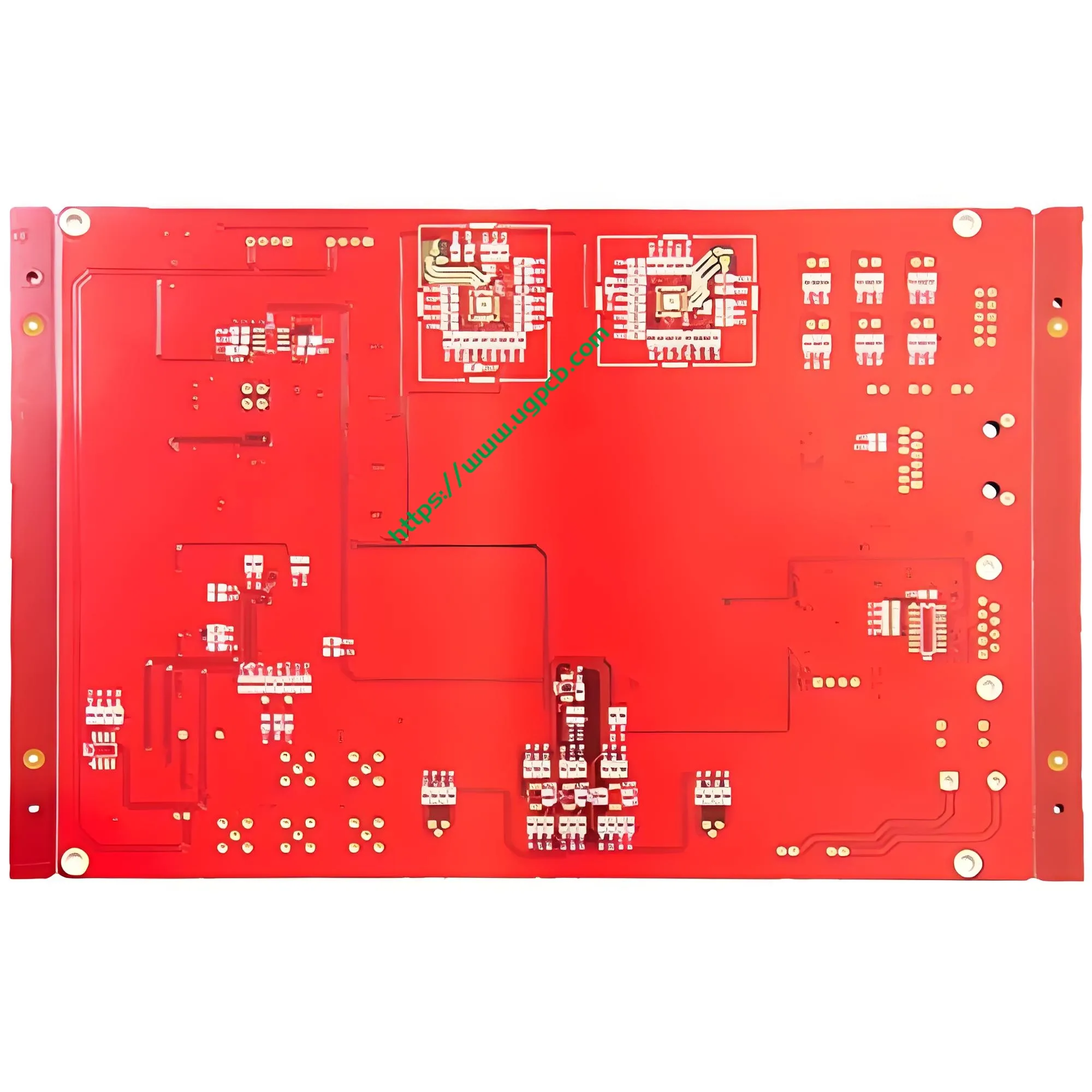
I. Descripción general del producto: PCB de precisión diseñada para equipos estéticos
El instrumento de depilación láser se basa en un sistema de control central.. Este sistema dicta la seguridad., estabilidad, y eficacia general del tratamiento. En el corazón de este sistema se encuentra elPCB de instrumento de depilación láser. Este componente es todo menos trivial..
La UGPCB presenta unaplaca de circuito impreso rígida de doble capa para este propósito exacto. Fabricamos este tablero utilizando un laminado epoxi reforzado con vidrio FR4 de alta calidad.. El espesor del tablero mide 1,0 mm.. Sus dimensiones compactas son 53.68 x 37,5 mm. Adaptamos específicamente estas especificaciones a las limitaciones de espacio interno de los dispositivos láser portátiles y profesionales modernos..
Este tarjeta de circuito impreso soporta ambos Luz pulsada intensa IPL y láser de diodo sistemas de depilación. Garantiza conexiones eléctricas estables y una transmisión de señal confiable.. un superior tarjeta de circuito impreso (Conjunto de placa de circuito impreso) Forma la base misma de los equipos estéticos de alto rendimiento.. UGPCB se especializa en ofrecer alta confiabilidad, Placas de circuitos de alta precisión para fabricantes mundiales de dispositivos de belleza..
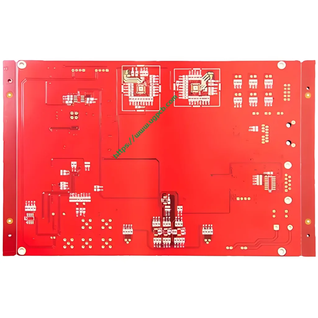
II. Definición del producto: ¿Qué es una PCB para instrumentos de depilación láser??
APCB de instrumento de depilación láser es una placa de circuito impreso dedicada. Gestiona funciones básicas como la distribución de energía., control del controlador láser, monitoreo de temperatura, e interacción con la interfaz de usuario.
Piense en ello como el sistema nervioso central del dispositivo.. Canaliza con precisión la energía eléctrica desde la batería al generador láser.. Monitorea simultáneamente la temperatura del sistema., ajusta los niveles de energía, y procesa las entradas de los botones.
Técnicamente, este producto es unde dos caras, PCB rígido con orificio pasante chapado. Utiliza material FR4. Según IPC-6012 (Especificación de calificación y rendimiento para tableros impresos rígidos), Esta tabla se adapta al tipo rígido con agujeros chapados.. Nuestro producto cumpleClase 2 requisitos (Productos electrónicos de servicio dedicado). Esta clase se adapta a dispositivos donde la alta confiabilidad es esencial pero no de misión crítica., como sistemas de depilación para uso doméstico y de salón.
III. Elementos esenciales del diseño: Precisión de ingeniería
El excelente diseño de PCB va mucho más allá de la simple conectividad. Nuestro equipo de ingeniería se centra en varios factores críticos para esta PCB de depilación láser..
3.1 Diseño de aislamiento y antiinterferencias.
Los instrumentos de depilación láser contienen circuitos controladores de alto voltaje y circuitos de control de bajo voltaje.. Interferencia electromagnética (EMI) entre estos dominios a menudo causa inestabilidad. UGPCB aísla físicamente los bucles de alimentación y señal. Utilizamos una acumulación de capas racional y un enrutamiento optimizado para mitigar la interferencia mutua de manera efectiva..
3.2 Diseño compacto y optimización del espacio
El 53.68 x El tamaño de 37,5 mm exige una integración de alta densidad. Nuestro equipo de diseño logra una ubicación integral del módulo funcional dentro de este espacio limitado.. Este enrutamiento denso garantiza un rendimiento eléctrico excelente al tiempo que permite la miniaturización del dispositivo..
3.3 Gestión Térmica
Los circuitos del controlador láser generan un calor considerable durante el funcionamiento.. La PCB actúa como vía primaria de conducción de calor.. FR4 ofrece conductividad térmica inherente. Combinado con vertido de cobre optimizado y colocación térmica., Nuestro diseño disipa el calor de manera eficiente.. Este enfoque aumenta la confiabilidad del dispositivo y extiende la vida útil operativa..
3.4 Adhesión a los estándares de diseño IPC
IPC-2221 (Norma genérica sobre diseño de tableros impresos) recomienda un espacio eléctrico mínimo de 0,1 mm (4 mils) para equipos generales. Nuestro diseño utiliza un ancho de línea y un espaciado de0.36milímetros y 0,38 mm. Esta especificación supera con creces el requisito mínimo.. Proporciona un margen de seguridad sustancial para el rendimiento eléctrico..
IV. Principio de trabajo: Cómo la PCB impulsa la emisión láser
El principio de depilación láser es sencillo., sin embargo, un control preciso requiere una compleja coordinación de PCB. Todo el flujo de trabajo sigue estos pasos.:
Paso 1: Entrada y gestión de energía. La batería o el adaptador suministra energía bruta.. El circuito de administración de energía de la PCB regula, filtros, y distribuye esta energía. Proporciona limpieza, voltaje estable a todos los módulos funcionales.
Paso 2: Control de nivel de energía. El usuario selecciona un nivel de energía. (comúnmente 5 ajustes ajustables). La MCU (Unidad de microcontrolador) en la PCB recibe este comando. Luego envía un PWM (Modulación de ancho de pulso) señal. Esta señal impulsa con precisión el circuito del controlador láser., Ajustar la corriente de salida al generador láser..
Paso 3: Conducción y emisión de láser. El circuito controlador convierte la energía eléctrica en una corriente operativa precisa para el diodo láser.. Esta corriente hace que el láser emita la longitud de onda específica. (normalmente 808 nm o 1064 nm).
Paso 4: Monitoreo y protección en tiempo real. Los sensores de temperatura en la PCB monitorean continuamente el estado térmico del dispositivo. La MCU reduce automáticamente la energía o apaga la salida si las temperaturas exceden los umbrales seguros. La PCB también maneja funciones de detección de contacto con la piel y recuento de disparos.. Toda esta lógica compleja se ejecuta a la perfección en el 53.68 x tablero de 37,5 mm.
V. Aplicaciones principales y escenarios de uso
Nosotros diseñamos esto.PCB de depilación láser para diversas aplicaciones en la industria estética.
| Campo de aplicación | Caso de uso específico | Equipo típico |
|---|---|---|
| Cuidado de belleza en el hogar | depilación personal | Dispositivos IPL de uso doméstico, sistemas láser domésticos |
| Salones Profesionales | Servicios de estética comercial. | Equipo láser de diodo de calidad profesional |
| Estética Médica | Tratamientos clínicos | Sistemas de terapia con láser médico |
| Fabricación ODM/OEM | Producción por contrato | Conjunto de PCB de dispositivo depilatorio de marca |
Además, La lógica de diseño y los procesos de fabricación de esta PCB son adaptables.. Se adaptan a otros dispositivos estéticos., incluidomáquinas de fotorrejuvenecimiento, removedores de pigmentación, y RF (radiofrecuencia) instrumentos de belleza.
VI. Clasificación de productos
Podemos clasificar científicamente este producto en múltiples dimensiones.:
- Por material de sustrato: PCB rígido de tela de vidrio epoxi FR4
- Por recuento de capas: 2-capa (tablero rígido estándar de doble cara)
- Por acabado superficial: ACEPTAR (Oro de inmersión de níquel químico) / Proceso de chapado en oro
- Por clasificación de inflamabilidad: UL 94 V-0 grado retardante de llama
- Por aplicación: Medicina del consumidor / PCB de dispositivo estético
- Por nivel de rendimiento IPC-6012: Clase 2 (Productos electrónicos de servicio dedicado)
VII. Composición de materiales: Garantía de calidad FR4
7.1 Laminado revestido de cobre FR4
Fabricamos este PCB usandoLaminado revestido de cobre epoxi-vidrio FR4. FR4 es el sustrato predominante en la industria de PCB. Consiste en tejido de fibra de vidrio impregnado con resina epoxi., curado bajo alta temperatura y presión. Para IPC-4101 (Especificación de Materiales Base para Tableros Impresos Rígidos y Multicapa), FR4 exhibe estas propiedades críticas:
- Temperatura de transición vítrea (tg): 130–140°C
- Constante dieléctrica (Dk): 4.3–4,8 a 1MHz
- Calificación de inflamabilidad: Cumple con UL 94 V-0
- Coeficiente de expansión térmica (CTE): 12–18 ppm/°C
Específicamente, según IPC-4101/21, Las placas FR-4 estándar tienen una Tg (método MAT) desde 110°C hasta 135°C. UGPCB selecciona materiales que superan cómodamente esta línea base.
7.2 Lámina de cobre
Aplica UGPCB35/35µm (1oz/1oz) lámina de cobre en ambos lados. La especificación de 1 oz representa el espesor de cobre más utilizado.. Logra un equilibrio óptimo entre capacidad de transporte de corriente y rentabilidad..
7.3 Máscara de soldadura y tinta de leyenda
Aplicamos unmáscara de soldadura roja (aceite rojo) combinado conpersonajes serigrafiados en blanco (texto blanco) . Este esquema de alto contraste ofrece varias ventajas.. Facilita la inspección óptica automatizada (AOI). También ayuda a la inspección manual., rehacer, y mantenimiento. Además, la máscara protege los restos de cobre de la oxidación, bermudas, y puentes de soldadura durante el montaje.
VIII. Parámetros técnicos y cumplimiento de normas
8.1 Resumen de parámetros clave
| Parámetro | Especificación | Observaciones |
|---|---|---|
| Materia prima | FR4 | Laminado de tela de vidrio epoxi |
| Grosor del tablero | 1.0milímetros | Espesor rígido estándar |
| Recuento de capas | 2 capas | Enrutamiento de doble cara |
| Dimensiones | 53.68 x 37,5 mm | Factor de forma compacto |
| Apertura mínima | 0.33milímetros (aprox. 13 mils) | Capacidad de perforación de precisión |
| Ancho de línea / Espaciado | 0.36milímetros / 0.38milímetros (14.2/15 mils) | Supera los requisitos de autorización IPC-2221 |
| Espesor de lámina de cobre | 35/35µm (1oz/1oz) | Cobre pesado de doble cara |
| Acabado superficial | ACEPTAR (Oro de inmersión de níquel químico) | Proceso de chapado en oro |
| Color de máscara de soldadura | Rojo | aceite rojo |
| Color de leyenda | Blanco | Texto blanco |
8.2 Cumplimiento de estándares
El diseño y fabricación de nuestros productos siguen estrictamente estos estándares internacionales.:
- IPC-6012: Cualificación y rendimiento del tablero impreso rígido.
- IPC-4101/21: Especificación del material laminado FR-4
- IPC-A-600: Aceptabilidad de los tableros impresos.
- IPC-4552: Especificación de acabado superficial ENIG
- UL 94 V-0: Clasificación de inflamabilidad más alta para materiales plásticos.
8.3 Validación de fiabilidad
Para IPC-6012, Los tableros rígidos deben pasar varias pruebas de consistencia de calidad.. UGPCB realiza 100% pruebas electricas (sonda voladora o pruebas de dispositivos dedicados) en cada tablero. Este proceso garantiza una integridad eléctrica impecable antes del envío.. Nuestros tableros pasan consistentemente:
- Pruebas eléctricas: Continuidad, resistencia de aislamiento, voltaje soportado dieléctrico
- Pruebas mecánicas: Fuerza de pelado, alabeo, estabilidad dimensional
- Pruebas ambientales: Estrés térmico, ciclos de temperatura, resistencia a la humedad
IX. Características estructurales y características físicas.
9.1 Configuración de doble capa
Este2-PCB de capa Cuenta con circuitos de cobre en los lados superior e inferior del sustrato FR4.Orificios pasantes chapados (PTH) Proporcionar interconexión eléctrica entre las capas.. Esta estructura logra una alta densidad de enrutamiento mientras controla los costos de fabricación.. Representa el tipo de PCB más rentable para electrónica de consumo..
9.2 Apertura mínima 0,33 mm
La apertura mínima de 0,33 mm. (13 mils) demuestra la UGPCBcapacidad de perforación de precisión. IPC-6012 exige un estricto control de tolerancia y un espesor de revestimiento adecuado dentro de la pared del orificio. Nuestro proceso garantiza que estas especificaciones se cumplan consistentemente, garantizando la confiabilidad a largo plazo de las conexiones plateadas.
9.3 Precisión de ancho/espaciado de línea (0.36/0.38milímetros)
El ancho de pista de 0,36 mm y el espacio libre de 0,38 mm ofrecen márgenes sustanciales de seguridad eléctrica.. Comparado con la línea base IPC-2221 de 0,1 mm, Nuestro diseño reduce la diafonía y elimina los riesgos de cortocircuito.. Este enrutamiento conservador pero preciso mejora la integridad de la señal en entornos ruidosos de alta potencia..
9.4 Ventajas del Acabado Superficial ENIG
adoptamosOro de inmersión de níquel químico (ACEPTAR) para tratamiento de superficies, Totalmente compatible con IPC-4552. Este proceso de chapado en oro ofrece distintos beneficios.:
- Soldabilidad superior: La capa de oro protege el níquel de la oxidación., garantizando una excelente formación de juntas de soldadura.
- Coplanaridad plana: ENIG proporciona una superficie excepcionalmente lisa, ideal para ensamblaje de componentes de paso fino.
- Vida útil extendida: El recubrimiento resiste la oxidación., permitiendo el almacenamiento a largo plazo sin degradación del rendimiento.
- Compatibilidad de unión de cables de aluminio: Este acabado se adapta a requisitos específicos de embalaje de alta gama..
IPC-4552 especifica un espesor de capa de níquel de 3 a 6 µm y un espesor mínimo de capa de oro de 0,05 µm. El proceso ENIG de UGPCB cumple estrictamente con estas especificaciones.
incógnita. Flujo del proceso de fabricación
Producir una PCB de depilación láser de alta calidad requiere un riguroso, flujo de trabajo de varios pasos. La UGPCB sigue esta secuencia precisa:
- Corte: Cortamos los grandes paneles revestidos de cobre FR4 en piezas manejables de tamaño de producción.
- Perforación: taladradoras CNC crear todos los agujeros pasantes, incluyendo las aperturas de precisión de 0,33 mm.
- Deposición de cobre no electrolítica & Revestimiento de paneles: Depositamos químicamente una fina capa de cobre dentro de los agujeros.. Este proceso crea el barril conductor de PTH., permitiendo la conexión entre capas.
- Transferencia de patrones: laminamos, exponer, y revelar una película fotorresistente para transferir el patrón del circuito a las superficies de cobre.
- Aguafuerte: El grabado químico elimina el cobre no deseado, dejando el patrón del circuito final con un ancho de traza preciso de 0,36 mm.
- Aplicación de máscara de soldadura: Aplicamos la tinta de máscara de soldadura roja.. Este recubrimiento protege los circuitos y define las almohadillas de soldadura expuestas..
- Acabado superficial (ACEPTAR): Aplicamos las capas de níquel químico y oro por inmersión., Totalmente compatible con IPC-4552.
- Impresión de leyendas: Imprimimos la leyenda serigrafiada en blanco., marcar claramente los designadores de componentes y los indicadores de polaridad.
- Prueba eléctrica: realizamos 100% sonda voladora o pruebas eléctricas basadas en accesorios para verificar el rendimiento.
- Enrutamiento / Corte en V: Enrutamos o cortamos en V el panel de producción hasta el final 53.68 x dimensión de 37,5 mm.
- Control de calidad final & Embalaje: Inspeccionamos las placas según los criterios IPC-A-600.. Los tableros aceptados se empaquetan al vacío para protegerlos durante el envío..
XI. ¿Por qué elegir UGPCB para la PCB de su instrumento de depilación láser??
11.1 Respaldo estándar autorizado
UGPCB se alinea estrictamente con IPC-6012, IPC-4101, IPC-A-600, y estándares IPC-4552. Cada proceso, desde la selección del material hasta la inspección final, sigue puntos de referencia verificables de la industria. Nuestra calidad resiste las más estrictas auditorías.
11.2 Fabricación de precisión avanzada
Nuestra capacidad para producir aperturas mínimas de 0,33 mm y un ancho/espaciado de línea de 0,36/0,38 mm destaca nuestra experiencia técnica.. Contamos con la precisión necesaria para aplicaciones exigentes de depilación láser..
11.3 Profunda experiencia en la industria estética
UGPCB posee un amplio conocimiento en el campo de los PCB para dispositivos estéticos. Entendemos íntimamente los requisitos únicos del láser., IPL, y equipos de fotorrejuvenecimiento, incluido el aislamiento de alto voltaje, gestión térmica, Supresión de EMI, y estrictas restricciones de confiabilidad.
11.4 UL 94 V-0 Garantía de inflamabilidad
Obtenemos materiales que cumplen con losUL 94 V-0 Clasificación: la clasificación retardante de llama más alta.. Según UL94, V-0 Requiere que cada muestra se queme durante ≤10 segundos después de cada aplicación de llama.. El tiempo total de combustión para un conjunto de cinco muestras debe ser ≤50 segundos.. Además, No hay gotas de llamas que puedan encender el algodón subyacente.. Esto garantiza la máxima seguridad., incluso en condiciones de funcionamiento anormales.

XII. Contáctenos para su solución de PCB personalizada
UGPCB ofrece alta calidadPCB para instrumentos de depilación láser y llave en manotarjeta de circuito impreso Servicios a fabricantes globales de dispositivos estéticos.. Somos tu socio ideal si lo estás:
- Un ingeniero de diseño que desarrolla sistemas de depilación de próxima generación.
- Un gerente de adquisiciones que busca un proveedor de PCB confiable.
- Un gerente de producto que requiere soluciones PCBA personalizadas.
- Un equipo emprendedor entrando al mercado de los dispositivos de belleza..
Contáctenos hoy para obtener una hoja de datos del producto, una cotización competitiva, o una consulta técnica gratuita!
📧 Correo electrónico: [info@ugpcb.com]
🌐 Sitio web: [www.ugpcb.com]
📞 Teléfono: [+86-135 4412 8719]
XIII. Declaración de fuente de datos
Los estándares técnicos y los datos de rendimiento citados en este artículo provienen de las siguientes instituciones autorizadas:
- PCI (Asociación que conecta industrias electrónicas) — Los estándares a los que se hace referencia incluyen IPC-6012 (Especificación de calificación y rendimiento para tableros impresos rígidos), IPC-4101 (Especificación de Materiales Base para Tableros Impresos Rígidos y Multicapa), IPC-A-600 (Aceptabilidad de los tableros impresos), IPC-2221 (Norma genérica sobre diseño de tableros impresos), y IPC-4552 (Especificación para níquel químico/oro por inmersión (ACEPTAR) Revestimiento para tableros impresos).
- UL (Laboratorios aseguradores) — UL 94 (Norma para pruebas de inflamabilidad de materiales plásticos para piezas de dispositivos y electrodomésticos) V-0 calificación de llamas.
- Publicaciones técnicas de la industria — Parámetros de propiedades del material FR4 (Tg 130–140°C, Dk 4,3–4,8 a 1 MHz, CET 12–18 ppm/°C) Son valores de referencia reconocidos de hojas de datos de materiales compuestos y directrices IPC-4101..













