

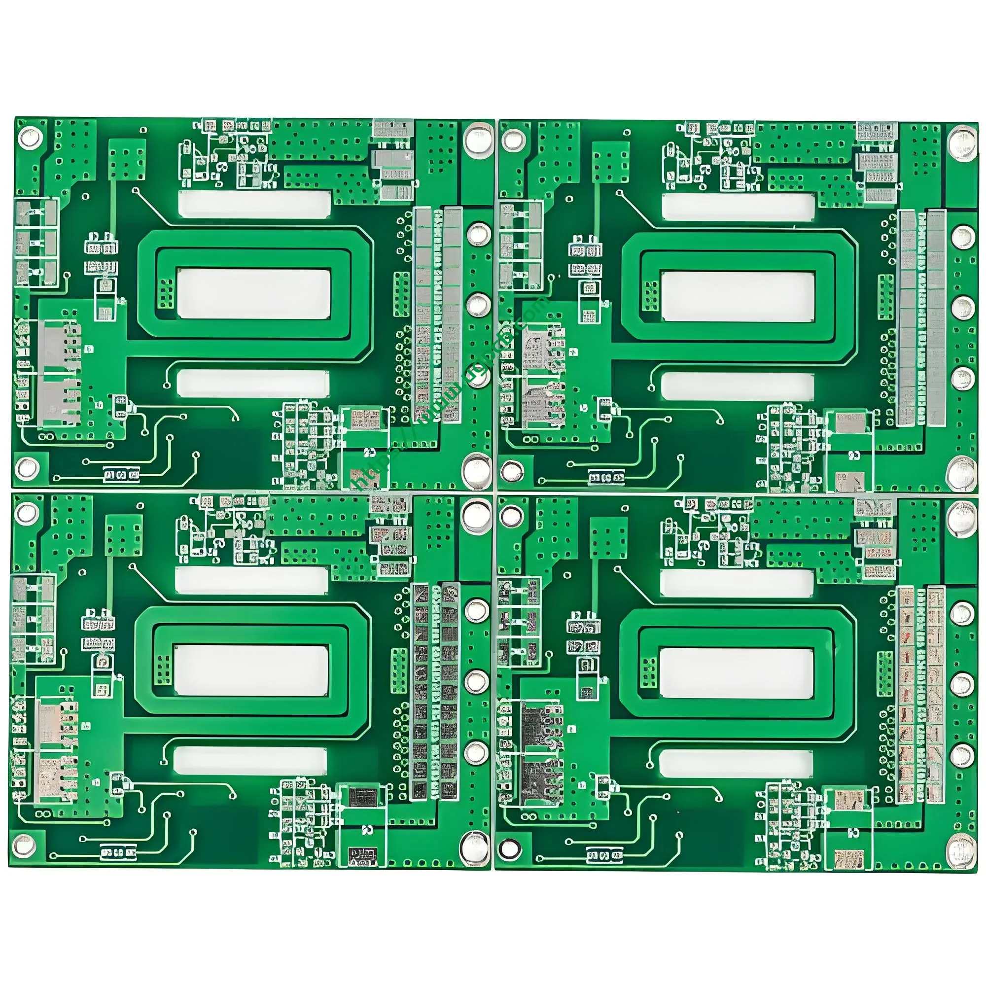
Descripción general del producto: ¿Qué es una PCB de doble cara de níquel-paladio-oro??
Una PCB de doble cara de níquel-paladio-oro (también conocido como PCB de doble cara ENEPIG) es un placa de circuito impreso que presenta el oro de inmersión de paladio no electrolítico de níquel electrolítico (ENÉPICO) Acabado superficial en ambos lados del tablero.. Este tratamiento superficial avanzado se basa en la estructura tradicional de PCB de doble cara agregando una capa de paladio entre los depósitos de níquel y oro., creando un acabado compuesto de tres capas robusto que ofrece una soldabilidad superior, rendimiento de unión de cables, y estabilidad ambiental.
La PCB de doble cara de níquel, paladio y oro de UGPCB utiliza el laminado revestido de cobre Kingboard KB6160A FR-4 como material base.. El tablero mide 49.6 × 32.8 mm con un espesor de 1.6 mm y un espesor de lámina de cobre de 1 onz (aproximadamente 35 μm). La máscara de soldadura es verde con caracteres serigrafiados en blanco.. Con una apertura mínima de 0.27 mm y un ancho/espaciado mínimo de línea de 0.27 × 0.3 milímetros, Esta PCB ENEPIG ofrece una fabricación de precisión combinada con un acabado superficial de alta calidad..
La PCB de níquel, paladio y oro es ampliamente reconocida como un "acabado superficial universal" en la industria electrónica.. Sirve para una amplia gama de aplicaciones., incluyendo telecomunicaciones, electrónica de consumo, controles industriales, sistemas de seguridad, electrónica automotriz, fuente de alimentación, dispositivos domésticos inteligentes, equipo medico, y sistemas militares/aeroespaciales.
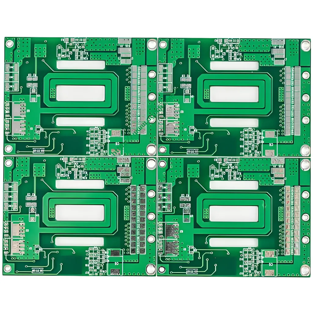
Especificaciones técnicas clave
| Parámetro | Especificación |
|---|---|
| Laminado | Placa King KB6160A FR-4 |
| Grosor del tablero | 1.6 milímetros |
| Número de capas | De dos caras |
| Tamaño de tablero | 49.6 × 32.8 milímetros |
| Apertura mínima | 0.27 milímetros |
| Ancho/espaciado mínimo de línea | 0.27 × 0.3 milímetros |
| Espesor de lámina de cobre | 1 onz (≈35 µm) |
| Acabado superficial | Níquel-Paladio-Oro (ENÉPICO) |
| Máscara de soldadura / Leyenda | Máscara de soldadura verde / Serigrafía blanca |
Detalles laminados: Laminado revestido de cobre KB6160A FR-4
KB6160A es un laminado revestido de cobre FR-4 de alto rendimiento fabricado por Kingboard Laminates Holdings Ltd.. Este material está diseñado específicamente para placas de cableado impresas a doble cara estándar. (PWB) fabricación. Cumple con la hoja de especificaciones IPC-4101/21. Las propiedades clave incluyen:
- Bloqueo UV (UVB) capacidad: Previene la transmisión de luz durante la toma de imágenes., mejorando la precisión y el rendimiento de la transferencia de patrones
- Excelente estabilidad dimensional: Garantiza la precisión durante todo el proceso de fabricación.
- Resistencia al calor y propiedades mecánicas superiores: Cumple con los requisitos de aplicaciones de alta confiabilidad
- Temperatura de transición vítrea (tg): 135°C (método DSC)
- Temperatura de descomposición térmica (td): 305°C (método TGA)
- CTE del eje z (A1/a2): 58 ppm/°C (< tg) / 286 ppm/°C (> tg)
- Constante dieléctrica (Dk): 4.58
- Factor de disipación (df): 0.022
- Resistividad de volumen: 1 × 10⁸ MΩ-cm
- Absorción de humedad: 0.21%
- Calificación de inflamabilidad: UL94V-0
(Los datos anteriores provienen de la hoja de datos técnicos de Kingboard KB6160A., con métodos de prueba según los estándares de la serie IPC-TM-650.)
El acabado superficial ENEPIG: Una explicación detallada
¿Qué es ENEPIG??
ENEPIG significa Níquel electrolítico, Paladio electrolítico, Oro por inmersión. Es un tratamiento superficial químico no electrolítico que deposita secuencialmente tres capas metálicas: níquel, paladio, y oro, en el circuito de cobre de un tarjeta de circuito impreso.
La estructura tricapa de ENEPIG está formada por:
- Capa inferior: níquel no electrolítico (En): Espesor de 3 a 5 μm. Esta capa actúa como barrera de difusión., Previene la migración de cobre a la superficie y al mismo tiempo proporciona soporte mecánico y una base para soldar..
- Capa intermedia: paladio no electrolítico (PD): Espesor de 0,05 a 0,1 μm. Esta capa de barrera crítica evita la interacción entre el níquel y el oro., eliminando la corrosión galvánica.
- Capa Superior – Oro de Inmersión (au): Espesor de 0,03 a 0,05 μm. Esta fina capa proporciona una excelente soldabilidad y protección contra la oxidación..
Según IPC-4556A (lo último 2025 revisión), Los requisitos de espesor de depósito de ENEPIG se especifican de la siguiente manera:
- capa de níquel: 3 μm en 6 μm (medido en promedio ± 4σ)
- capa de paladio: 0.05 μm en 0.30 μm (medido en promedio ± 4σ)
- capa de oro: Mínimo 0.030 μm, máximo 0.07 μm (medido por debajo del promedio − 4σ)
(Las especificaciones de espesor anteriores se basan en IPC-4556A., Especificación para níquel químico/paladio químico/oro de inmersión (ENÉPICO) Revestimiento para tableros impresos.)
El flujo del proceso ENEPIG
Los PCB de doble cara de níquel, paladio y oro de UGPCB siguen un proceso de revestimiento no electrolítico estandarizado:
Desengrasado → Micrograbado → Inmersión previa → Activación → Niquelado electrolítico → Chapado de paladio electrolítico → Chapado en oro por inmersión → Secado
Cada paso del proceso incluye múltiples etapas de enjuague para garantizar la calidad y la adhesión del revestimiento.. Las reacciones químicas involucradas incluyen tanto reacciones de oxidación-reducción como reacciones de desplazamiento..
Ventajas principales de los PCB de doble cara de níquel-paladio-oro
1. Eliminación completa del defecto de la “almohadilla negra”
La ENIG (Oro de inmersión de níquel químico) El proceso ha estado plagado durante mucho tiempo por el defecto "Black Pad", una condición en la que el ataque del oro a la capa de níquel provoca uniones de soldadura quebradizas y fallas prematuras.. ENEPIG soluciona este problema introduciendo una capa barrera de paladio entre el níquel y el oro, Previniendo el contacto directo y eliminando la corrosión del límite de grano.. Los datos de la industria muestran que ENEPIG reduce la aparición de almohadillas negras en casi 90% comparado con ENIG. En condiciones de ciclos de temperatura extrema, ENEPIG demuestra hasta 30% mayor confiabilidad que ENIG.
2. Capacidad superior de unión de cables
Los acabados superficiales ENEPIG ofrecen un excelente rendimiento de unión para alambres de oro y aluminio.. La capa de paladio amplía la ventana del proceso para la unión de alambres de oro, permitiendo uniones de cables confiables incluso con depósitos de oro más delgados. En muchas aplicaciones, ENEPIG admite resistencias de unión de cables que exceden 10 gramos para uniones de alambre de oro y aluminio. Esto hace que los PCB de doble cara de níquel, paladio y oro sean especialmente adecuados para aplicaciones de ensamblaje híbrido y embalaje de semiconductores que requieren unión de cables..
3. Excelente soldabilidad y tolerancia al reflujo múltiple
Los acabados superficiales de ENEPIG proporcionan una excelente soldabilidad con soldaduras con y sin plomo. (incluyendo aleación SAC305). Los PCB con acabado ENEPIG pueden soportar hasta 10 Ciclos de reflujo sin degradación significativa..
4. Vida útil extendida
Gracias a la capa protectora de paladio., Los acabados superficiales ENEPIG ofrecen una resistencia superior a la oxidación y la corrosión.. Esto se traduce en una vida útil significativamente más larga en comparación con otros acabados superficiales.. Según las directrices del IPC, Los acabados superficiales ENEPIG pueden alcanzar la categoría IPC 3 vida útil de al menos doce meses.
5. Mayor flexibilidad de diseño
A diferencia de los procesos electrolíticos de níquel-oro, ENEPIG es un proceso no eléctrico que no requiere barras colectoras ni cables enchapados.. Esto permite procesar más tableros simultáneamente en el mismo baño de revestimiento., aumentar el rendimiento general. Además, ENEPIG no impone restricciones de ruta, proporcionando mayor flexibilidad para diseños de circuitos de alta densidad.
Cómo funcionan los PCB de doble cara de níquel-paladio-oro
La acción sinérgica de tres capas de revestimiento
El rendimiento excepcional de los PCB de doble cara de níquel-paladio-oro se debe a la sinergia precisa de las tres capas de revestimiento.:
① Capa de níquel (Aleación Ni-P) – La barrera de la fundación
La capa de níquel sirve como base de la estructura ENEPIG.. Su función principal es bloquear la difusión del átomo de cobre a la superficie., prevenir la formación de compuestos intermetálicos frágiles de Cu-Sn (IMC) durante la soldadura o la exposición a altas temperaturas. El espesor del níquel normalmente se controla entre 3 y 6 μm., con contenido de fósforo estrictamente mantenido entre 7% y 9% para equilibrar la dureza y la resistencia a la corrosión.
② Capa de paladio (PD) – La barrera crítica y la capa de activación
La capa de paladio es la característica definitoria que distingue a ENEPIG de ENIG.. Actúa como un “muro divisorio,“Previene la migración y la corrosión de los límites de grano entre el níquel y el oro.. La capa de paladio debe ser lo suficientemente gruesa como para bloquear la difusión del níquel a la superficie del oro y evitar la corrosión excesiva del depósito de níquel no electrolítico..
③ Capa de oro (au) – Protección y Soldabilidad
La fina capa exterior de oro protege el níquel de la oxidación al mismo tiempo que proporciona una baja resistencia al contacto y una excelente soldabilidad.. Porque la capa de paladio proporciona aislamiento., la capa de oro en ENEPIG se puede hacer más delgada (0.03–0,05 µm) sin comprometer la confiabilidad, lo que ayuda a reducir los costos de material en cierta medida.
Clasificación de PCB de doble cara de níquel-paladio-oro
La PCB de doble cara de níquel-paladio-oro de UGPCB se puede clasificar científicamente en múltiples dimensiones:
Por número de capas
- PCB de doble cara: Los circuitos conductores se distribuyen a ambos lados del sustrato., con conexiones eléctricas establecidas a través de orificios pasantes chapados (PTH).
Por material base
- Laminado de tela de vidrio epoxi FR-4: Usando Kingboard KB6160A, Cumple con IPC-4101/21.
Por acabado superficial
- ENÉPICO (Níquel electrozados con electricidad de oro de paladio) : Estructura de revestimiento compuesto de tres capas..
Por dominio de aplicación
- PCB de uso general de alta confiabilidad: Apto para telecomunicaciones, electrónica automotriz, dispositivos medicos, aeroespacial, controles industriales, y más.
Por precisión de fabricación
- PCB de precisión: Apertura mínima de 0.27 milímetros, ancho/espaciado mínimo de línea de 0.27 × 0.3 milímetros.
Flujo del proceso de fabricación
La producción de PCB de doble cara de níquel, paladio y oro de UGPCB sigue un flujo de trabajo de fabricación integral:
Escenario 1: Preparación del sustrato
- Corte de material: El laminado revestido de cobre KB6160A se corta a las dimensiones requeridas.
- Perforación: Perforación mecánica con una apertura mínima de 0.27 milímetros.
- Deposición de cobre no electrolítica & Revestimiento de paneles: Metalización por orificios.
Escenario 2: Formación de circuitos
- Transferencia de patrones: Laminación con película seca → Exposición → Revelado.
- Grabado de circuito: Eliminación del exceso de cobre para formar el patrón del circuito..
- AOI (Inspección óptica automatizada) : Garantizar la precisión del circuito.
Escenario 3: Máscara de soldadura y leyenda
- Impresión de máscara de soldadura: Aplicación de tinta verde para proteger circuitos y evitar puentes de soldadura..
- Impresión de leyendas: Personajes serigrafiados en blanco..
Escenario 4: Acabado superficial (ENÉPICO)
- Desengrasante: Eliminación de contaminantes de la superficie..
- Micrograbado: Grabado ligero de la superficie de cobre para mejorar la adhesión..
- Inmersión previa: Pretratamiento antes de la activación..
- Activación: Deposición de una capa de semilla de paladio catalítico sobre cobre..
- Niquelado no electrolítico: Deposición de capa de níquel. (3–5 µm).
- Recubrimiento de paladio no electrolítico: Deposición de capa de paladio. (0.05–0,1 µm).
- Chapado en oro por inmersión: Deposición de capa de oro. (0.03–0,05 µm).
- El secado: Finalización del acabado superficial..
Escenario 5: Inspección final
- Prueba eléctrica: Garantizar la continuidad eléctrica y el aislamiento..
- Inspección visual: Comprobación de la calidad de la superficie.
- Embalaje & Envío.
Aplicaciones típicas
Los PCB de doble cara de níquel, paladio y oro de UGPCB se utilizan ampliamente en numerosas industrias:
Equipos de telecomunicaciones
- Estaciones base, enrutadores, interruptores
- Módulos de comunicación de alta frecuencia., dispositivos de radiofrecuencia
Electrónica automotriz
- Unidades de control del motor (CUBRIR)
- Sistemas de infoentretenimiento en el vehículo
- ADA (Sistemas avanzados de asistencia al conductor)
- Bms (Sistemas de gestión de baterías) para vehículos de nueva energía

Dispositivos médicos
- Dispositivos médicos implantables
- Instrumentos de diagnóstico, equipo de monitorización de pacientes
Aeroespacial & Defensa
- Electrónica de naves espaciales y satélites.
- Sistemas de control de aviación.
Controles Industriales & Seguridad
- SOCIEDAD ANÓNIMA (Controladores lógicos programables)
- Accionamientos de motores industriales
- Equipos de seguridad y vigilancia.
Electrónica de Consumo & Inicio inteligente
- Placas base para teléfonos inteligentes
- Módulos de control del hogar inteligente
- Dispositivos portátiles
Militar & Electrónica de potencia
- Sistemas electrónicos militares.
- Módulos de potencia, convertidores de potencia
¿Por qué elegir UGPCB para PCB de doble cara de níquel-paladio-oro??
✅ Cumplimiento de los estándares IPC
Los PCB de doble cara de níquel, paladio y oro de UGPCB se fabrican estrictamente de acuerdo con IPC-4556A.. El laminado KB6160A cumple con IPC-4101/21, asegurando una estandarización completa desde el material base hasta el acabado de la superficie.
✅ Capacidades de fabricación de precisión
Con una apertura mínima de 0.27 mm y ancho/espaciado mínimo de línea de 0.27 × 0.3 milímetros, UGPCB satisface las demandas de interconexión de alta densidad (IDH) y ensamblaje de componentes de paso fino.
✅ Garantía de alta confiabilidad
El acabado superficial ENEPIG reduce los defectos de las almohadillas negras en casi 90% y entrega hasta 30% Mayor confiabilidad que ENIG bajo fluctuaciones extremas de temperatura.. Los productos resisten múltiples ciclos de reflujo y cumplen con J-STD-003 Categoría 3 requisitos de durabilidad.
✅ Soporte técnico profesional
El equipo de UGPCB brinda soporte técnico durante todo el proceso., desde la revisión de archivos Gerber y la optimización de BOM hasta el ensamblaje de PCBA.
Consultas & Realizar pedidos
Listo para convertir su diseño en una PCB de doble cara de níquel-paladio-oro de alta calidad?
📧 Correo electrónico: ventas@ugpcb.com
📞 Teléfono: +86-135 4412 8719
🌐 Sitio web: www.ugpcb.com
📋 Proceso de pedido:
- Enviar archivos Gerber, lista de materiales, y documentación de diseño.
- El equipo de ingeniería de la UGPCB realiza DFM (Diseño para la fabricación) revisar.
- Confirmación de pedido y calendario de entrega..
- Fabricación y control de calidad..
- Seguimiento de envíos y logística.
Si necesitas Prototipos de PCB o producción en volumen, UGPCB se compromete a ofrecer PCB de doble cara de níquel, paladio y oro de alta calidad y servicios técnicos profesionales..
Declaración de fuente de datos
Los datos técnicos y las especificaciones estándar citadas en este documento provienen de las siguientes organizaciones autorizadas:
- IPC-4556A: Especificación para níquel químico/paladio químico/oro de inmersión (ENÉPICO) Revestimiento para tableros impresos (2025 revisión)
- IPC-4101/21: Especificación de Materiales Base para Tableros Impresos Rígidos y Multicapa – la hoja de especificaciones aplicable a KB6160A
- Hoja de datos técnicos de Kingboard KB6160A (Kingboard Laminados Holdings Ltd.)
- IPC-TM-650: Manual de métodos de prueba – los métodos de prueba estándar utilizados para las mediciones de propiedades de materiales
- J-ETS-003: Pruebas de soldabilidad para tableros impresos – el estándar de prueba de soldabilidad
- UL94: Norma para pruebas de inflamabilidad de materiales plásticos para piezas de dispositivos y electrodomésticos – estándar de clasificación de inflamabilidad
Todos los datos citados anteriormente provienen de las normas oficiales y documentos técnicos enumerados., Garantizar precisión y autoridad..













